
Optical waveguide fabrication

a technology of optical waveguides and fabrication methods, which is applied in the direction of glass making apparatus, lasers, instruments, etc., can solve the problems of non-standard requirements, high cost of equipment, and inability to produce waveguides with the required high power properties, etc., and achieve the effect of improving the transparency of the core layer

Active Publication Date: 2014-09-30
STATE OF ISRAEL - SOREQ NUCLEAR RES CENT
View PDF5 Cites 0 Cited by
  • Summary
  • Abstract
  • Description
  • Claims
  • Application Information

AI Technical Summary

Benefits of technology

The patent text describes a way to make a layer more transparent by heating it with a laser beam. This can be useful in improving the performance of certain devices.

Problems solved by technology

Waveguide fabrication does not require fiber drawing, which requires non-standard, costly equipment and brings limitations to the possible designs.
None of the above mentioned techniques has the ability to produce a waveguide with the required high power properties.
Thus high power waveguide lasers have not been realized until now.

Method used


Image

  • Optical waveguide fabrication
  • Optical waveguide fabrication
  • Optical waveguide fabrication

Examples


Embodiment Construction

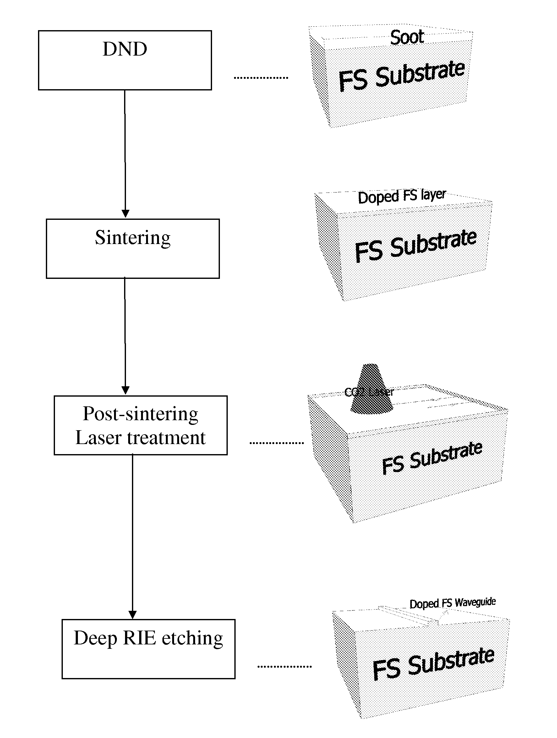
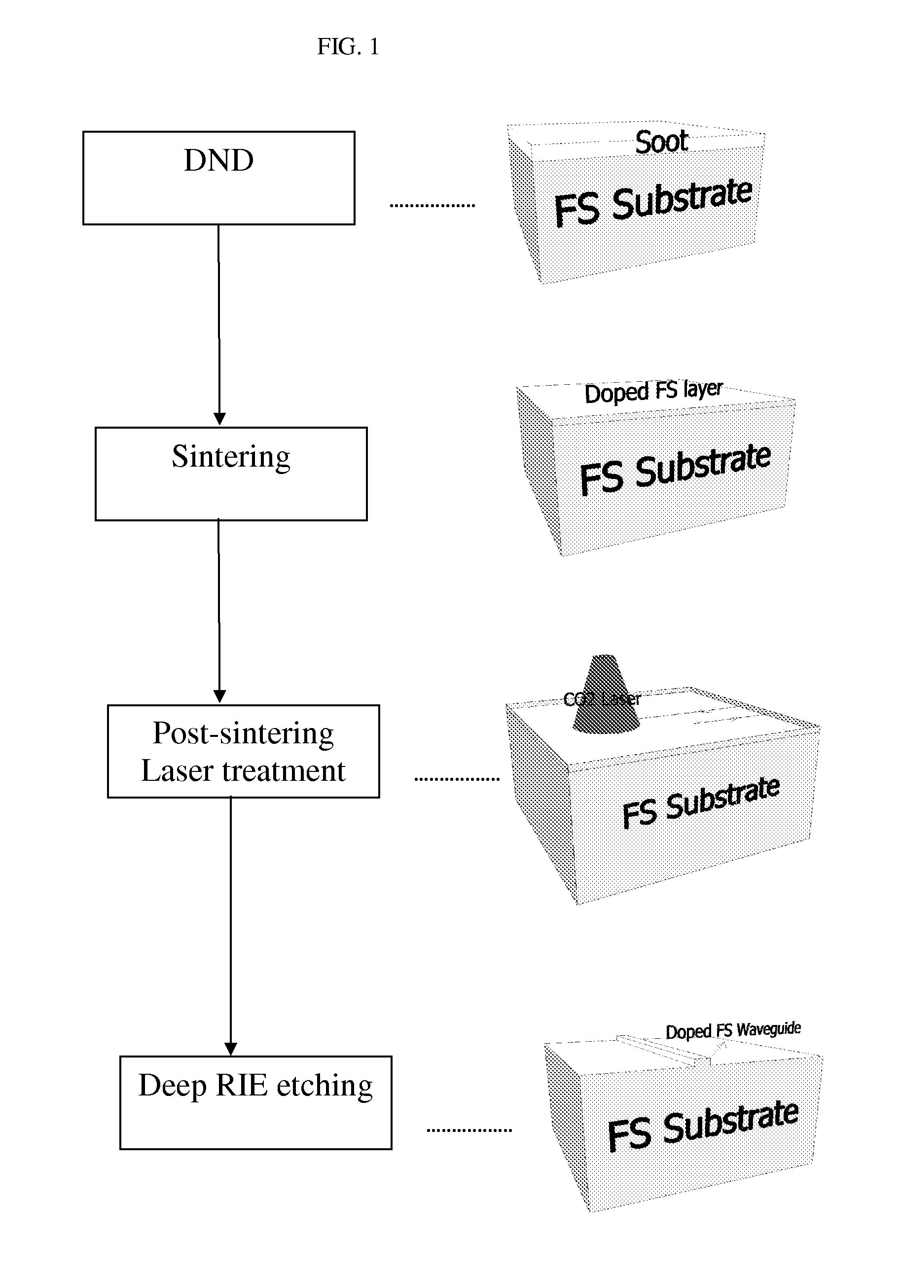
[0025]In accordance with a non-limiting embodiment of the present invention, there is provided a method for producing a silica waveguide including the following steps (shown in FIG. 1):

[0026]a. Silica deposition

[0027]b. Sintering

[0028]c. Post Sintering Laser Treatment

[0029]d. Deep Reactive Ion Etching (DRIE)

[0030]a. Deposition Process for Thick Active Waveguides:

[0031]Depositing a layer (coating) of doped silica nanoparticles on a fused silica (FS) substrate (e.g., by flame hydrolysis deposition on a silica glass substrate). The process is similar to that used for fibers; however, the thickness of the coating is much lower. Typically the after-sintering layer thickness is between 5 and 50 μm. Layer thickness is defined as the final thickness of the material after all thermal processes. The layer may be co-doped with a dopant that modifies the refractive index of the material to provide optical guiding in the layer, such as aluminium, boron and other dopants well-known in the art of ...


PUM

PropertyMeasurementUnit
thicknessaaaaaaaaaa
thicknessaaaaaaaaaa
surface roughnessaaaaaaaaaa

Abstract

An optical device including an active core layer of silica glass doped with ions which serve as optical emitters, the active core layer being on a silica glass substrate and having a layer thickness of at least 5 μm, and wherein the layer is sintered at a temperature range of 1500-1600 C. and subsequently heat treated by a laser.

Description

CROSS REFERENCE TO OTHER APPLICATIONS[0001]This application is a U.S. national phase application of PCT patent application PCT / US2011 / 033862, filed Apr. 26, 2011, which claims priority from U.S. Provisional Patent Application 61 / 328,137, filed Apr. 27, 2010.FIELD OF THE INVENTION[0002]The present invention relates generally to a method of fabricating an optical waveguide.BACKGROUND OF THE INVENTION[0003]High power silica fiber lasers are used for material processing (cutting welding) and numerous other applications. In principle, the fibers are made of a core and clad. The core is doped with rare earth ions for lasing media.[0004]Light is typically transmitted by means of total reflection due to a difference of optical refractive indices between the clad and the core. Both the fiber core and cladding are typically doped elements such as germanium dioxide (GeO2) or aluminium oxide (Al2O3)) are added to the silica core to slightly increase the optical refractive index. The aluminium a...

Claims


Application Information

Patent Timeline
Patent Type & Authority Patents(United States)
IPC IPC(8): G02B6/10C03B37/022G02B6/13G02B6/136H01S3/063H01S3/16H01S3/17
CPCG02B6/13H01S3/063H01S3/1618H01S3/176G02B6/136
Inventor ATAR, GILBRUNER, ARIELEGER, DAVIDSFEZ, BRUNO
Owner STATE OF ISRAEL - SOREQ NUCLEAR RES CENT
Learn More