
Method for the fabrication of optical waveguide devices in photonic crystal fibers and in waveguides with hollow structures

a technology of optical waveguides and photonic crystal fibers, which is applied in the manufacture of tools, cladded optical fibres, instruments, etc., can solve the problems of insufficient state of the art and structural challenges of fabrication, and achieve the effect of increasing losses

Active Publication Date: 2019-06-25
OZ OPTICS
View PDF9 Cites 0 Cited by
  • Summary
  • Abstract
  • Description
  • Claims
  • Application Information

AI Technical Summary

Benefits of technology

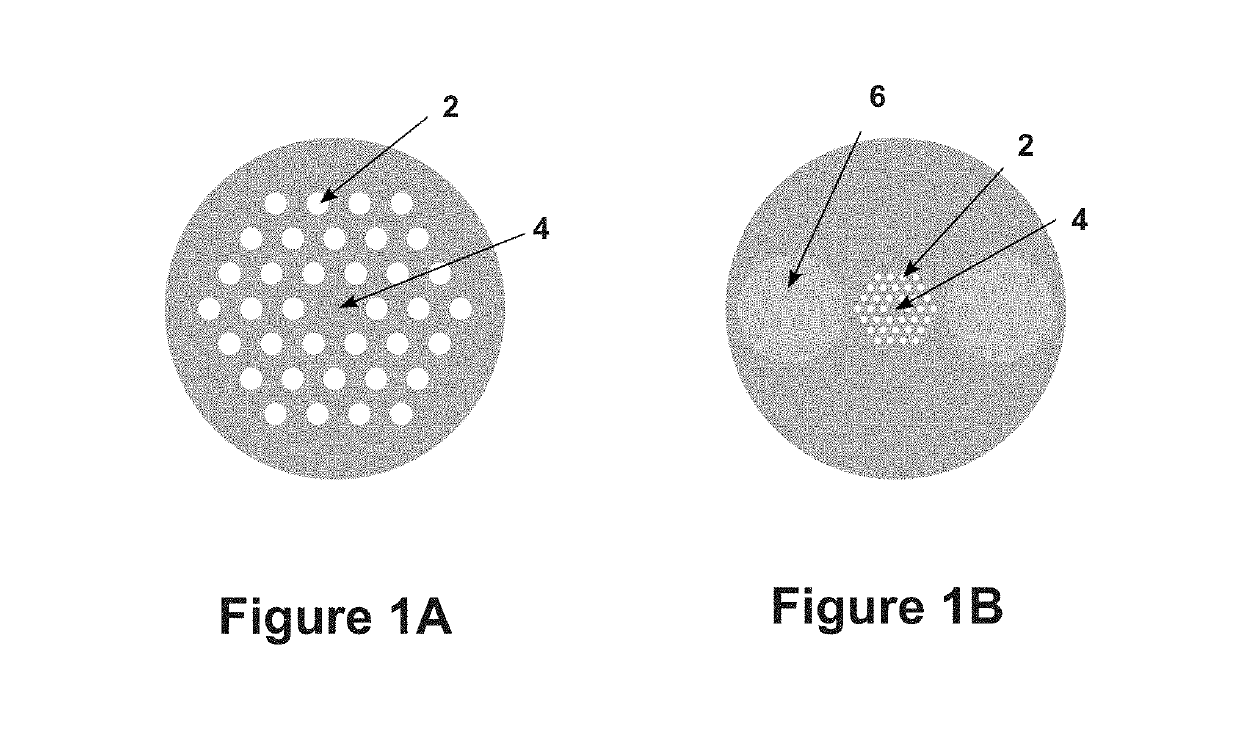
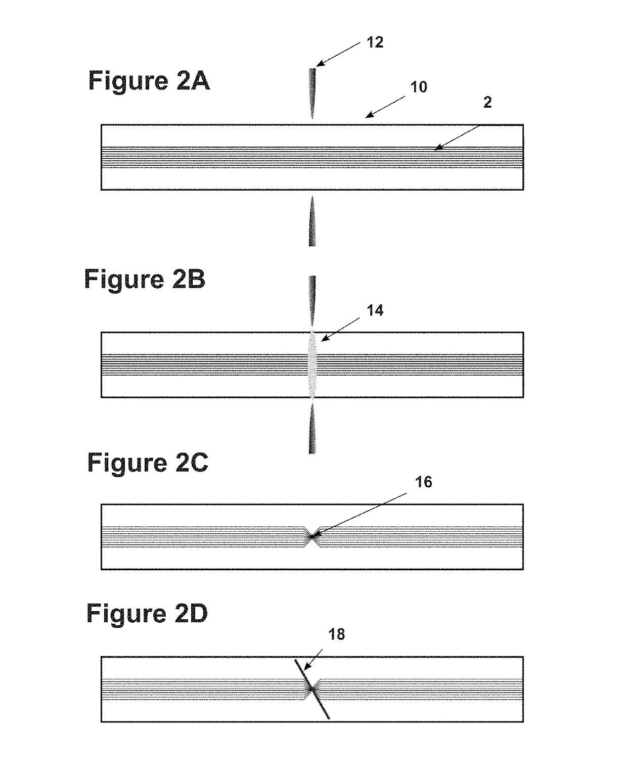
[0006]In one aspect of the present invention is a method of pre-modification of a photonic crystal fiber (PCF) in order to create local disruption in the band gap core and allow for the coupling of waveguide devices from the fiber core to the fiber cladding using the femtosecond laser fabrication method. This local pre-modification can be accomplished, for example, by using a finely tuned source of heat, such as electrical arc discharge, to locally collapse the hollow holes in a small region of the PCF. Fine control is recommendable in order to obtain a disruption in the fiber large enough to enable efficient coupling to waveguides in the cladding but small enough to avoid complete destruction of the fiber itself or otherwise create significantly higher losses that would defeat the original device purpose or render the device unusable.

Problems solved by technology

However these structures also present a challenge for the fabrication of waveguides with femtosecond lasers.
Since there is no material to be modified inside those holes, the methods that form the current state of the art are not adequate and the introduction of other non-obvious elements to the fabrication procedures are required in order to have a means to achieve the same potential for the local creation of devices as is currently possible in standard optical fibers with femtosecond laser writing.

Method used


Image

  • Method for the fabrication of optical waveguide devices in photonic crystal fibers and in waveguides with hollow structures
  • Method for the fabrication of optical waveguide devices in photonic crystal fibers and in waveguides with hollow structures

Examples


Embodiment Construction

[0011]One embodiment of the present invention consists of a method to couple light from the core of a photonic crystal optical fiber. or other waveguide device with hollow structure, to its cladding in order to use that light for any purpose leading to the fabrication of a functional optical device. A femtosecond laser can be used to produce a region of modified index of refraction that forms a waveguide. However, that index modified region is not sufficient when the principle operation of the fiber is a photonic band gap that has the fiber core surrounded by hollow (air filled) elements, as such regions remain unaffected by the femtosecond laser writing system. In order to locally disturb the fiber core light confinement, one aspect of the present method includes a preparation step that selectively heats, and partially or completely collapses the hollow structures, opening the way for femtosecond written waveguides to couple light from the fiber core into the cladding or to escape ...


PUM

PropertyMeasurementUnit
structureaaaaaaaaaa
heataaaaaaaaaa
radiiaaaaaaaaaa

Abstract

There is provided a method to fabricate optical taps and waveguide devices in photonic crystal fibers and other fibers with hollow structures. The method involves a preparation step, where the hollow holes inside the fiber are collapsed or partially modified locally; and a waveguide fabrication step, where a femtosecond laser is focused inside the fiber and used to produce optical waveguides that interact in the region that was previously modified in the preparation step.

Description

CROSS REFERENCE TO RELATED APPLICATIONS[0001]The present application claims priority to Canadian Application No. 2,897,130 filed Jul. 14, 2015, the content of which is incorporated by reference in its entirety.TECHNICAL FIELD[0002]The present invention relates to the fabrication of optical waveguides inside photonic crystal optical fibers and in waveguides with hollow structures using focused femtosecond laser radiation and fiber fusion by heating.BACKGROUND OF THE INVENTION[0003]Co-owned U.S. Pat. No. 7,295,731 B2 describes a method for using femtosecond laser radiation for the creation of optical waveguiding devices inside standard optical fibers. The femtosecond laser is focused inside the optical fiber and the intense light generated in the focal region produces non-linear absorption in the glass fiber and creates permanent refractive index changes. The different refractive index regions can be used to produce waveguide vias for light to travel, thus functionalizing the fiber fo...

Claims


Application Information

Patent Timeline
Patent Type & Authority Patents(United States)
IPC IPC(8): C03B37/012C03B37/15B23K26/53B23K26/60G02B6/02C03C25/6208G02B6/28G02B6/255
CPCC03C25/6208B23K26/53B23K26/60C03B37/15G02B6/2852G02B6/02309G02B6/2552G02B6/02147G02B6/02314G02B6/02323
Inventor SEZERMAN, OMURFERNANDES, LUIS ANDREBEST, GARLANDNG, MI LIKANE, SAIDOU
Owner OZ OPTICS
Learn More