Waveguide manufacturing process

a manufacturing process and waveguide technology, applied in the field of optoelectronics, can solve the problems of diffusion loss, non-linear effect loss, mainly diffuse loss, etc., and achieve the effect of reducing the roughness of the waveguide flanks, low optical loss, and reducing the absorption loss of the waveguide manufactured by the method according to the invention

Active Publication Date: 2022-01-25
COMMISSARIAT A LENERGIE ATOMIQUE ET AUX ENERGIES ALTERNATIVES
View PDF13 Cites 0 Cited by
  • Summary
  • Abstract
  • Description
  • Claims
  • Application Information

AI Technical Summary

Benefits of technology

[0017]The first material is typically different from the second material. The epitaxy of the first material on the pattern the etching flanks of which are smoothed beforehand advantageously makes it possible to further reduce the roughness of the flanks. The optical diffusion losses in such a waveguide are thus reduced.
[0019]The method according to the invention thus makes it possible to manufacture different types of waveguides, for example a strip waveguide or an edge waveguide, while still minimising the roughness of the flanks of the waveguide. The method according to the invention makes it possible to manufacture waveguides that have very low optical losses by diffusion.
[0020]The epitaxy of the first material also makes it possible to limit and even suppress the impurities within this first material, which typically forms the core of the waveguide. The absorption losses of the waveguide manufactured by the method according to the invention are reduced.

Problems solved by technology

There are also losses due to non-linear effects, involving for example a two-photon absorption or by free carriers.
There are also diffusion losses that occur mainly at the flanks of the waveguide.
These diffusion losses are in particular linked to the roughness of the flanks.

Method used


Image

  • Waveguide manufacturing process
  • Waveguide manufacturing process
  • Waveguide manufacturing process

Examples


first embodiment

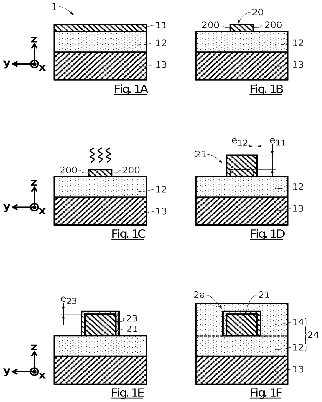
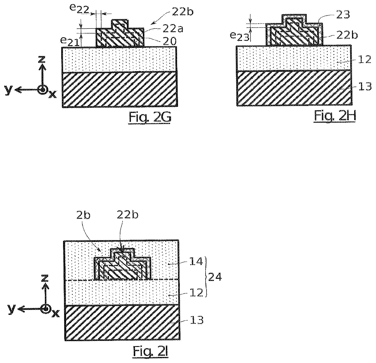
[0073]Preferably, an encapsulation of the core is then carried out by an encapsulation layer 14 (FIG. 1F). This encapsulation layer 14 is preferably made of SiO2. It can be deposited via CVD. It makes it possible to form another portion of the clad of the waveguide. The clad 24 is thus formed all around the core by the layers 12 and 14 made of SiO2. This first embodiment makes it possible to form a strip waveguide 2a.

[0074]In order to form a strip waveguide 2a that is single-mode at the wavelengths used in telecommunications (for example about 1.55 μm), the core 21 can have a height along z comprised between 0.2 μm and 0.4 μm, and a width along y comprised between 0.2 μm and 0.4 μm. The lower portion of the clad 24 formed by the layer 12 preferably has a height greater than or equal to 0.7 μm in a single-mode waveguide 2a configuration.

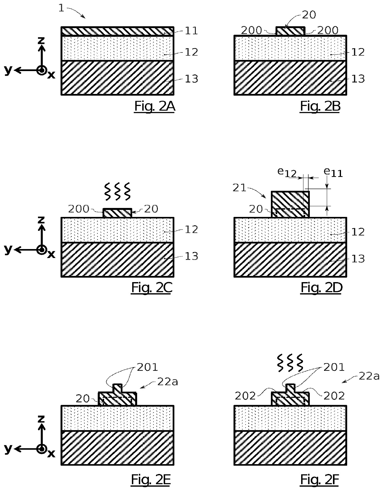
[0075]Other embodiments of the method according to the present invention can be considered. These embodiments can typically combine several sequence...

second embodiment

[0082]This second embodiment makes it possible to form an edge waveguide 2b.

[0083]The waveguides manufactured by the method according to the present invention can advantageously be used for LiDAR and 400G long-distance telecom applications, and for quantum photonics and frequency comb applications.

[0084]The invention is not limited to the embodiments described hereinabove and extends to all the embodiments covered by the claims.

[0085]In particular, several steps of etching and / or smoothing and / or epitaxy can be implemented to form the waveguide. In this case, the etching depths and / or the epitaxial thicknesses can vary from one step to another.


PUM

PropertyMeasurementUnit
thicknessaaaaaaaaaa
epitaxial thicknessaaaaaaaaaa
thicknessaaaaaaaaaa

Abstract

The invention relates to a method for manufacturing a waveguide (2a, 2b) comprising:A supplying of a substrate (1) comprising a stack of a first layer (11) based on a first material on a second layer (12) based on a second material, andat least one sequence successively comprising:An etching of the first material, in such a way as to define at least one pattern (20, 22a) having etching flanks (200, 201),A smoothing annealing assisted by hydrogen in such a way as to smooth the etching flanks (200, 201) of the at least one pattern (20, 22a),A re-epitaxy of the first material on the pattern (20, 22a) based on the first material.

Description

TECHNICAL FIELD[0001]The present invention relates to the field of optoelectronics. It has for particularly advantageous application the carrying out of waveguides that have very little optical losses by propagation.PRIOR ART[0002]In the field of silicon integrated optics, waveguides are essential components. They form an optical circuitry that makes it possible to interconnect different optoelectronic components. Sub-micrometric waveguides are in particular used in applications linked to optical telecommunications, photonics, non-linear optics and quantum computing.[0003]Waveguides generally comprise a core wherein light propagates and a clad that makes it possible to confine the light in the core, in contrast to refractive index. In order to improve the performance of sub-micrometric waveguides, it is important to reduce the optical losses caused during the propagation of the light within these waveguides.[0004]The optical losses are due to several physical phenomena. There are fo...

Claims


Application Information

Patent Timeline
Patent Type & Authority Patents(United States)
IPC IPC(8): G02B6/13G02B6/132G02B6/136G02B6/12H01L21/324
CPCG02B6/131G02B6/132G02B6/136G02B2006/1218G02B2006/12035G02B2006/12169G02B2006/12178H01L21/3247G02B2006/121
Inventor SCIANCALEPORE, CORRADOEL DIRANI, HOUSSEINHARTMANN, JEAN-MICHEL
Owner COMMISSARIAT A LENERGIE ATOMIQUE ET AUX ENERGIES ALTERNATIVES
Why Eureka
Try Eureka