Semiconductor on insulator structure made using radiation annealing

a technology of semiconductors and insulators, applied in the field of semiconductoroninsulator systems, methods and products of manufacture, can solve the problems of inability to meet the requirements of the application of the substrate, inability to meet the requirements of the substrate, etc., to achieve the effect of improving the overall manufacturing yield, and low step yield

Inactive Publication Date: 2009-08-25
CORNING INC
View PDF14 Cites 58 Cited by
  • Summary
  • Abstract
  • Description
  • Claims
  • Application Information

AI Technical Summary

Benefits of technology

[0018]The radiation annealing process heats at least part of the silicon layer to near or past its melting point, allowing at least part of the trapped hydrogen to escape, and healing the damage to the crystal lattice as the material cools. Furthermore, any roughness in the original surface is reduced, either from increased atom mobility at high temperature, or due to surface tension if the material is heated to a liquid state. Thus, with respect to the aforementioned drawbacks of CMP combined with furnace annealing (FA), the use of radiation anneal according to the present invention, such as by use of an excimer laser anneal (ELA) or microwave anneal, has the potential of overcoming the drawbacks of CMP and reducing the anneal time required for hydrogen outgassing.
[0021]The radiation wavelength should be selected to allow partial melting of the semiconductor layer. However, it is desirable that the bottom part of the crystalline layer is not melted. Therefore, the penetration depth of light into the semiconductor material should not be too large compared to the semiconductor layer thickness. As discussed below in reference to the Exemplary Data, energy densities per pulse above a threshold of approximately 800 mJ / cm2 at a wavelength of about 308 nm (XeCl laser) caused observable improvement in the surface roughness and in the crystalline quality when the crystalline silicon semiconductor layer thickness was approximately 500 nm. Each combination of semiconductor composition and thickness is expected to have its own energy threshold at which the desired effects are achieved. Therefore, using thinner semiconductor layers of silicon should reduce the energy threshold to below 800 mJ / cm2, while holding the other parameters constant.
[0026]The advantages of this invention are best understood after reading the detailed technical description, and in relation to existing SiOG processes. Nonetheless, the primary advantages of one or more embodiments of the present invention include: transfer of thinner silicon films; more uniform silicon films with higher crystal quality; faster manufacturing throughput; improved manufacturing yield; reduced contamination; and easy scalability to large substrates.
[0029]Improving manufacturing yield is also important for waste and cost reduction. By replacing two process steps with one, the overall manufacturing yield is expected to improve. This is particularly true if this polishing process has a low step yield, as anticipated. Although excimer laser crystallization of amorphous silicon films is known to have a low yield, the opposite is true in this particular case due to the single-crystal nature of the silicon. The process window is expected to be large because of the crystalline nature of the film, and therefore the yield is expected to be high.
[0031]The process is easily scalable to large areas. Excimer laser annealing is currently being applied to substrates up to 730 mm by 920 mm (Gen4) in size by display manufacturers. The substrate size can easily be increased as the substrate is scanned under the laser beam. This scalability potentially extends the product life as customer substrate size requirements increase. In contrast, surface polishing and furnace annealing become increasingly difficult for larger substrate sizes.

Problems solved by technology

The former two methods, epitaxial growth and wafer-wafer bonding, have not resulted in satisfactory structures in terms of cost and / or bond strength and durability.
(Due to the high temperature steps, this process is not compatible with lower-cost glass or glass-ceramic substrates.)
The resulting SOI structure just after exfoliation might exhibit excessive surface roughness (e.g., about 10 nm or greater), excessive silicon layer thickness (even though the layer is considered “thin”), unwanted hydrogen ions, and implantation damage to the silicon crystal layer (e.g., due to the formation of an amorphized silicon layer).
Lastly, the act of cleaving the silicon layer leaves a rough surface, which is known to cause poor transistor operation, so the surface roughness should be reduced to preferably less than 1 nm RA prior to device fabrication.
Disadvantageously, however, the CMP process does not remove material uniformly across the surface of the thin silicon film during polishing.
The above shortcoming of the CMP process is especially a problem for some silicon-on-glass applications because, in some cases, as much as about 300-400 nm of material needs to be removed to obtain a desired silicon film thickness.
Another problem with the CMP process is that it exhibits particularly poor results when rectangular SOI structures (e.g., those having sharp corners) are polished.
Indeed, the aforementioned surface non-uniformities are amplified at the corners of the SOI structure compared with those at the center thereof.
Still further, when large SOI structures are contemplated (e.g., for photovoltaic applications), the resulting rectangular SOI structures are too large for typical CMP equipment (which are usually designed for the 300 mm standard wafer size).
The CMP process, however, is costly both in terms of time and money.
The cost problem may be significantly exacerbated if non-conventional CMP machines are required to accommodate large SOI structure sizes.
However, high temperature anneals are not compatible with lower-cost glass or glass-ceramic substrates.
Lower temperature anneals (less than 700° C.) require long times to remove residual hydrogen, and are not efficient in repairing crystal damage caused by implantation.
Furthermore, both CMP and furnace annealing increase the cost and lower the yield of manufacturing.

Method used


Image

  • Semiconductor on insulator structure made using radiation annealing
  • Semiconductor on insulator structure made using radiation annealing
  • Semiconductor on insulator structure made using radiation annealing

Examples


examples

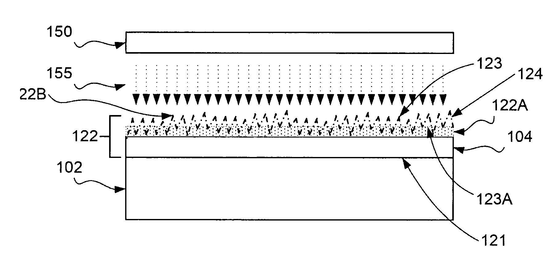
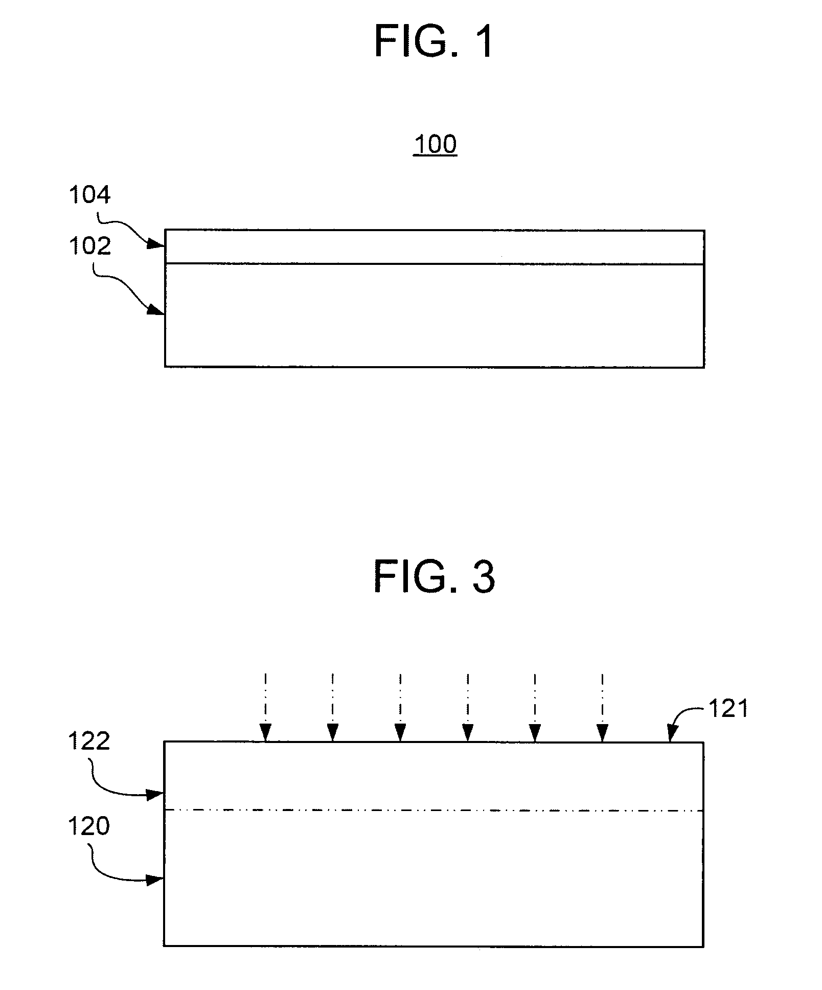
[0115]A series of experiments was conducted to demonstrate the applicability of the aforementioned laser annealing process on an SiOG structure. An SiOG structure 100 with a 500 nm thick silicon exfoliation layer 122 was exposed to radiation 155 of excimer laser 150 at 400-1250 mJ / cm2 for 1 to 100 pulses. The excimer laser 150 used was a XeCl Excimer Laser from Lambda Physik, operating at up to 100 Hz with 28 nsec pulses of 308 nm light. The penetration depth of 308 nm wavelength UV light into silicon is only a few nanometers, which results only in the melting of the top part of the silicon layer, if energy density of the laser beam on the silicon surface is properly chosen. The laser was used with an optical system, including homogenizers, to produce a uniform 5 mm×0.8 mm beam. Step-and-repeat exposure was used in the examples in the present application to expose areas larger than the beam size. Similar laser energies are sufficient to crystallize an amorphous silicon film, resulti...


PUM


Abstract

Systems and methods for and products of a semiconductor-on-insulator (SOI) structure including subjecting at least one unfinished surface to a laser annealing process. Production of the SOI structure further may include subjecting an implantation surface of a donor semiconductor wafer to an ion implantation process to create an exfoliation layer in the donor semiconductor wafer; bonding the implantation surface of the exfoliation layer to an insulator substrate; separating the exfoliation layer from the donor semiconductor wafer, thereby exposing at least one cleaved surface; and subjecting the at least one cleaved surface to the laser annealing process.

Description

CROSS-REFERENCE TO RELATED APPLICATION[0001]The present application claims benefit of the earlier filing date of U.S. Provisional Patent Application No. 60 / 809,881, filed on May 31, 2006, entitled “SEMICONDUCTOR ON INSULATOR STRUCTURE MADE USING RADIATION ANNEALING,” the content of which is relied upon and incorporated herein by reference in its entirety.FIELD OF THE INVENTION[0002]The present invention relates to the systems, methods and products of manufacture of a semiconductor-on-insulator (SOI) structure using improved processes, including radiation annealing, and in particular, laser annealing for finishing the semiconductor layer.BACKGROUND OF THE INVENTION[0003]To date, the semiconductor material most commonly used in semiconductor-on-insulator structures has been silicon. Such structures have been referred to in the literature as silicon-on-insulator structures and the abbreviation “SOI” has been applied to such structures. SOI technology is becoming increasingly important ...

Claims


Application Information

Patent Timeline
Patent Type & Authority Patents(United States)
IPC IPC(8): H01L27/01
CPCH01L21/268H01L21/76254H01L21/324H01L21/67115H01L21/7624H01L21/302G02F2202/09G02F2202/104H01L21/3247H01L21/00H01L21/762
Inventor COUILLARD, JAMES GREGORYLEHUEDE, PHILIPPEVALLON, SOPHIE A
Owner CORNING INC
Why Eureka
Try Eureka