

Semiconductor device
a technology of semiconductor devices and shielding films, which is applied in the direction of semiconductor devices, electrical equipment, transistors, etc., can solve the problems of deteriorating reliability of gate insulation films, inability to use, and inability to meet the requirements of us
- Summary
- Abstract
- Description
- Claims
- Application Information
AI Technical Summary
Benefits of technology
Problems solved by technology
Method used
Image

Examples
example 1
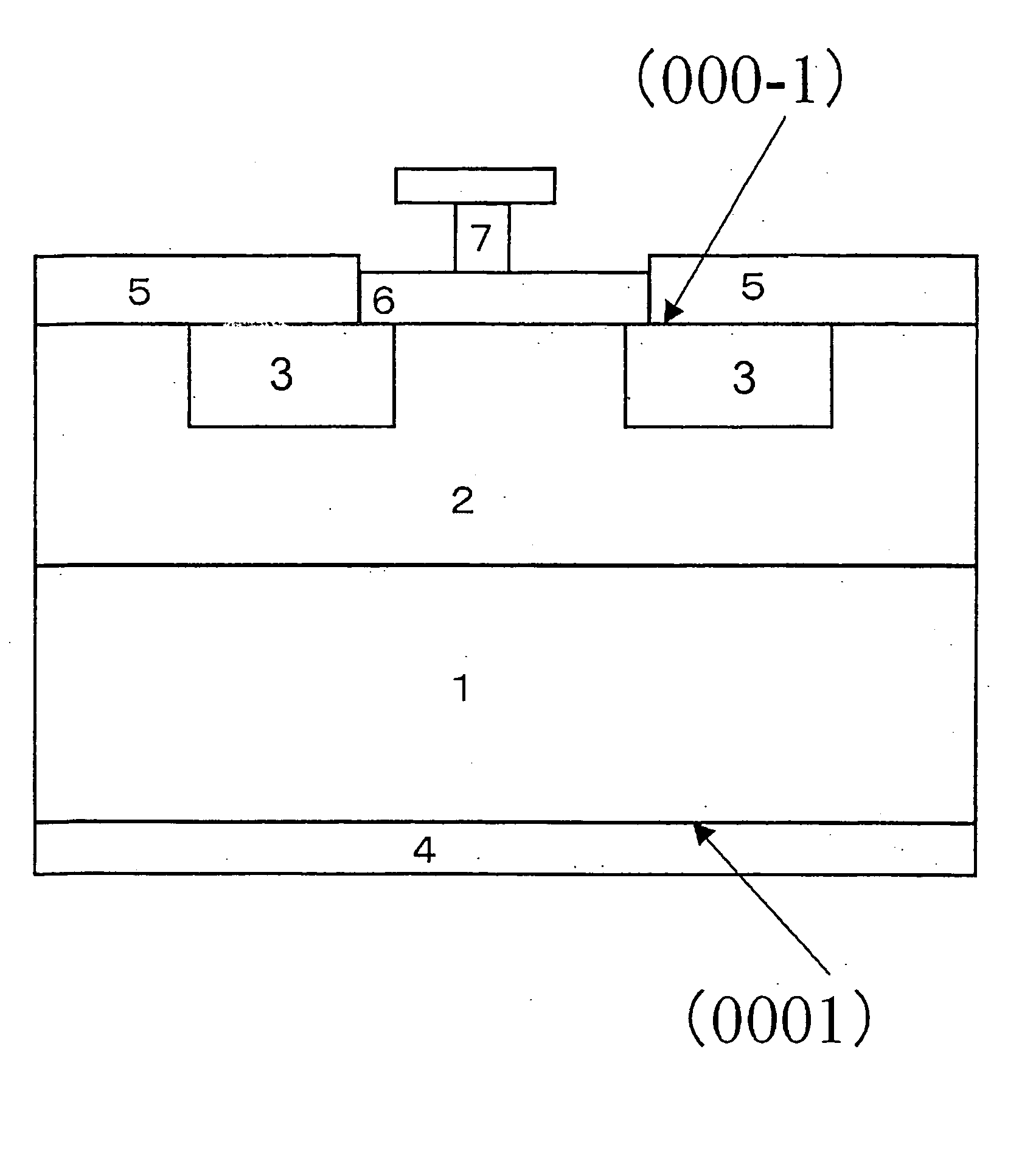
[0049]FIG. 1 is a schematic cross sectional view of a Schottky barrier diode as an example of the semiconductor device according to the present invention.
[0050] The Schottky barrier diode was prepared by a method set forth below.
[0051] (1) First, an N type epitaxial layer 2 was made to grow by 10 micrometers (μm) on the (000-1) face of an N type 4H—SiC bulk substrate 1 (resistivity: 0.002 ohm cm (Ω cm); thickness: 300 micrometers (μm)) by chemical vapor deposition (CVD) wherein nitrogen was used as impurities, and the concentration of the N type epitaxial layer 2 was 1×1016 cm3. The bulk substrate 1 and the epitaxial layer 2 formed a silicon carbide semiconductor area, and the top layer of the epitaxial layer 2 also served as the (000-1) face.
[0052] (2) In order to form a guard ring in the circumference section of the Schottky electrode 6, 1×1017 cm−3 of P type impurities made of aluminum or boron in the area where the guard ring of the epitaxial layer 2 was to be formed, was int...
example 2
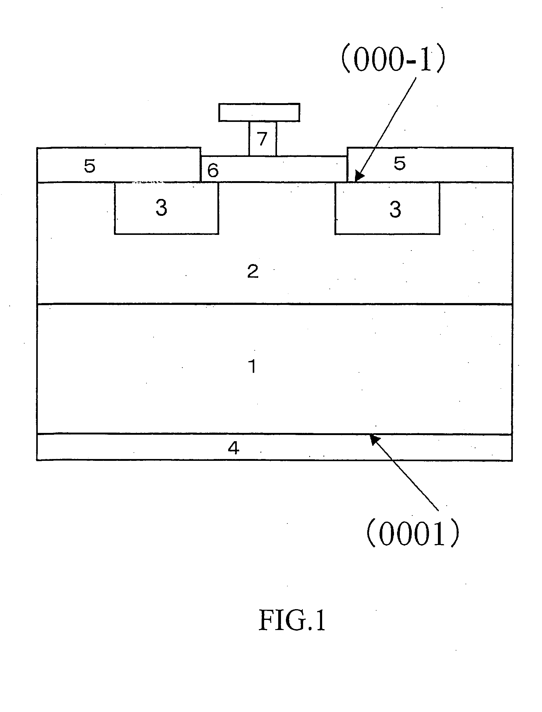
[0062]FIG. 2 is a cross sectional view of a lateral (Lateral resurf MOS structure) semiconductor device as a lateral MIS electric field effect device according to the present invention.
[0063] First, a 10-15 micrometer P type epitaxial layer 12 was formed on the (000-1) face of a P type 4H-SiC bulk substrate 11 (resistivity: 2 ohm cm (Ω cm); thickness: 300 micrometers(μm)) by chemical vapor deposition (CVD), wherein aluminum was used as impurities. The concentration of the P type impurities was 5×1015 cm−3. In this case, the SiC bulk substrate 11 may be an N type substrate.
[0064] The bulk substrate 11 and the epitaxial layer 12 form a silicon carbide semiconductor area, and the top layer of the epitaxial layer 12 also serves as the (000-1) face.
[0065] (2) Subsequently, an ion implantation mask for forming source areas and drain areas is formed with a thermally-oxidized film or SiO2 film by CVD (Chemical Vapor Deposition).
[0066] In this example, a LTO (Low Temperature Oxide) film ...
example 3
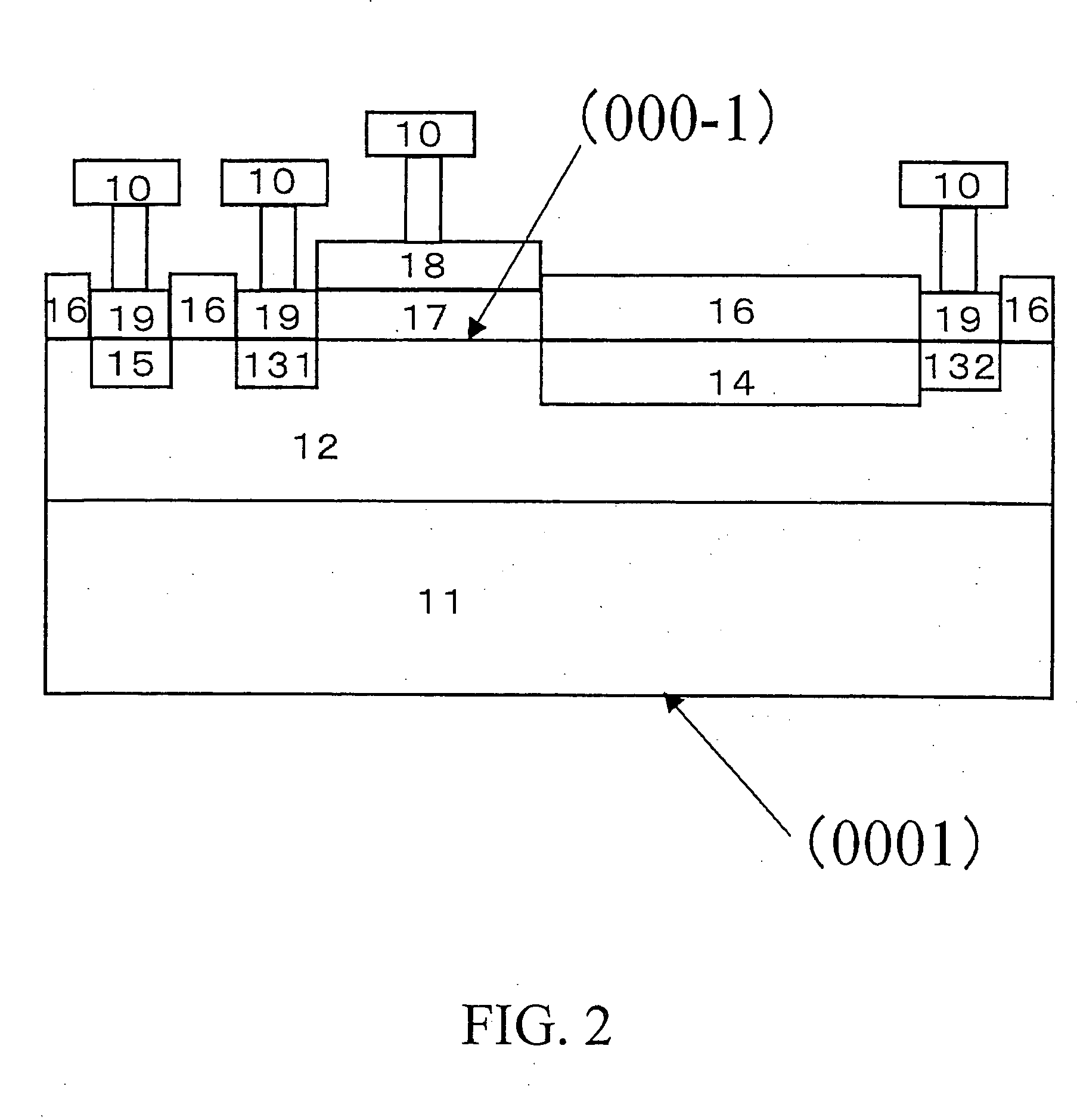
[0078]FIG. 3 is a cross sectional view of a lateral (Lateral resurf MOS structure) semiconductor device whose structure is different from that shown in FIG. 2 as an example of a lateral MIS electric field effect transistor according to the present invention.
[0079] Although the structure of the semiconductor device shown in FIG. 3 is basically the same as that shown in FIG. 2, they are different in terms that a P type impurity area 122 is formed on an epitaxial layer 12, and a source 131 and P+ type impurity area 15 are formed on the epitaxial layer 12.
[0080] The lateral Lateral resurf MOSFET semiconductor device shown in FIGS. 2 and 3 has a gate (comprising a gate insulation film and a gate electrode), a source, and a drain in the (000-1) face of a silicon-carbide semiconductor area, which is a switching element wherein on / off of current which flows in the (000-1) face between the source and the drain, is controlled by impressing voltage to the gate.
[0081] In addition, as an exam...
PUM
 Abstract
Description
Claims
Application Information