Tunnel field effect transistor and method of making the same

a field effect transistor and tunneling technology, applied in the direction of diodes, semiconductor devices, electrical apparatus, etc., can solve the problems of tfet performance and speed not meeting, vdd limit of 0.5v for regular cmoc scaling, and vdd limit of 0.5v for cmos transistors

Inactive Publication Date: 2016-11-17
QUALCOMM INC
View PDF7 Cites 24 Cited by
  • Summary
  • Abstract
  • Description
  • Claims
  • Application Information

AI Technical Summary

Benefits of technology

[0007]In some examples of the disclosure, the system, apparatus, and method for a vertical integrated tunnel field effect transistor, includes: a plurality of gate elements, each of the plurality of gate elements having a gate contact at one end thereof; a plurality of source or drain elements extending parallel to the plurality of gate elements and horizontally spaced therefrom; a plurality of fin elements extending parallel to the plurality of gate elements and vertically spaced therefrom, wherein each of the plurality of fin elements is horizontally spaced a first distance from each of the other ones of the plurality of fin elements; and a plurality of active gate regions, each of the plurality of active gate regions formed by an overlap of one of the plurality of gate elements and one of the plurality of fin elements, and wherein each of the plurality of active gate regions has a horizontal width larger than a vertical height.

Problems solved by technology

However, regular CMOC scaling runs into a Vdd limit of ˜0.5V and cannot further scale power substantially with traditional CMOS transistors.
However, TFET performance and speed cannot meet requirement in a System on Chip (SoC), such as a CPU block, or speed path because (1) future integrated SoCs will still have to meet ˜3 GHz CPU speed; a TFET cannot meet this requirement due to fundamentally lower Idsat and lower speed versus conventional CMOS at higher Vdd (˜0.5V); (2) SoCx can take advantage of the super low power of TFET for blocks and circuits functions that does not need high speed, but low power is the essential requirement; and (3) the industry needs an innovative solution that can meet both power and performance requirements for future SoCs to be effective alternatives.

Method used


Image

  • Tunnel field effect transistor and method of making the same
  • Tunnel field effect transistor and method of making the same
  • Tunnel field effect transistor and method of making the same

Examples


Embodiment Construction

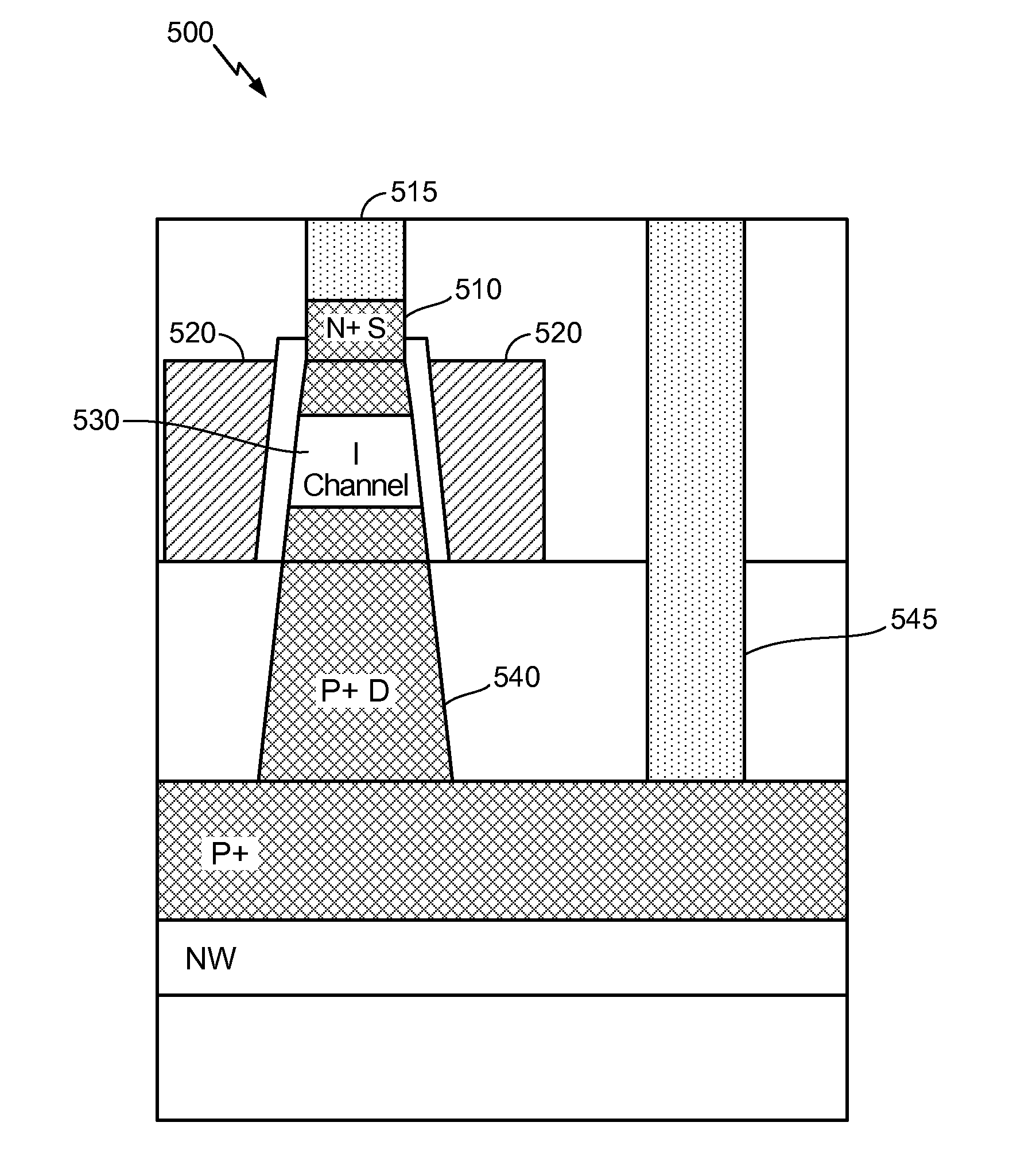
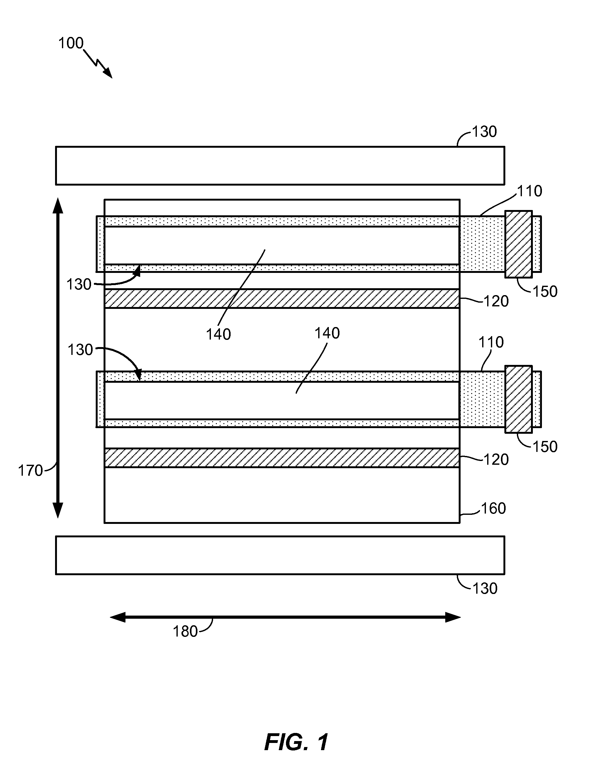
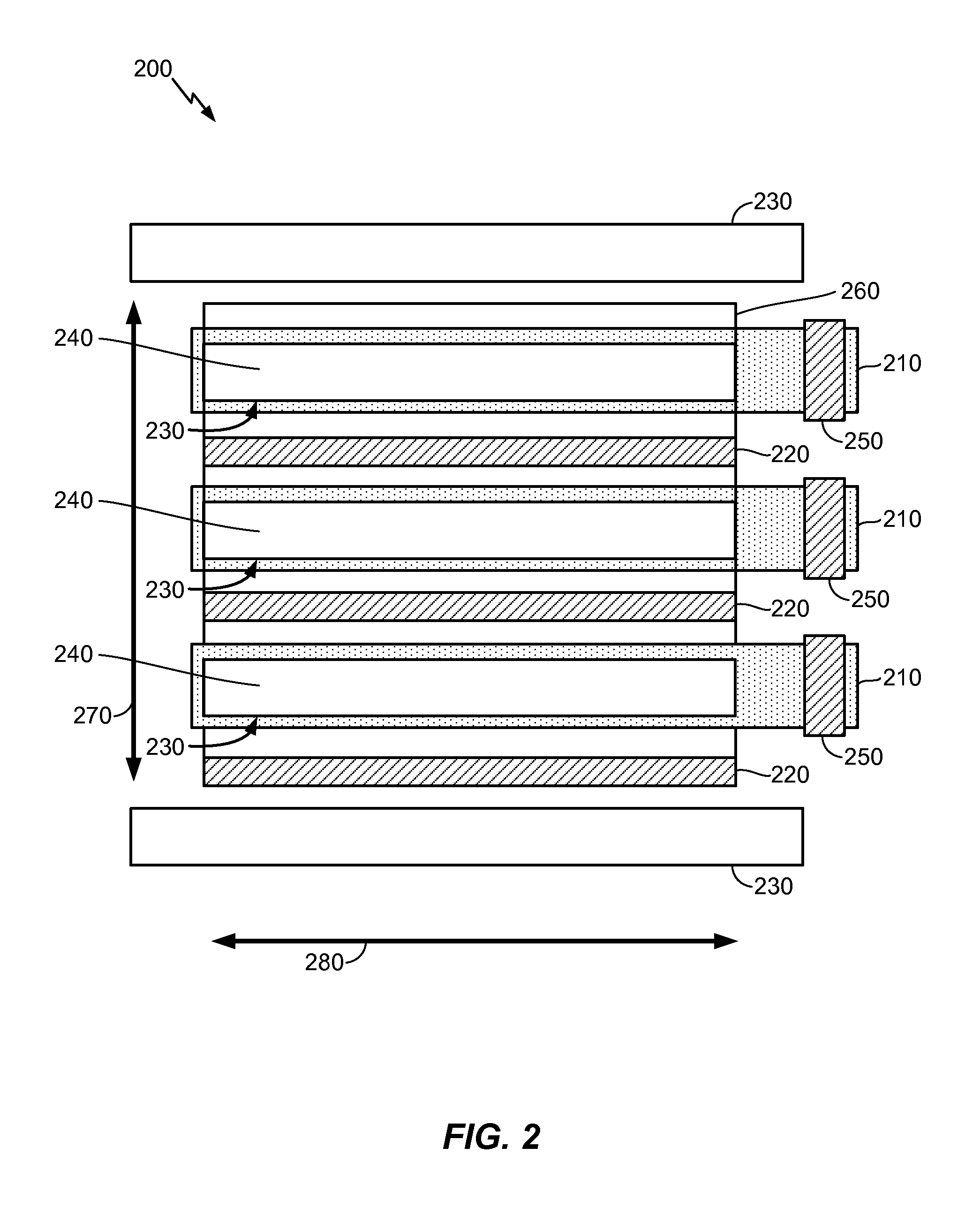
[0019]The exemplary methods, apparatus, and systems disclosed herein advantageously address the long-felt industry needs, as well as other previously unidentified needs, and mitigate shortcomings of the conventional methods, apparatus, and systems. For instance, the effective area of a transistor device according to one of the embodiments described herein may be increased by aligning the fin elements with the gate elements, which would improve the performance characteristics of the device.

[0020]The word “exemplary” is used herein to mean “serving as an example, instance, or illustration.” Any details described herein as “exemplary” is not necessarily to be construed as preferred or advantageous over other examples. Likewise, the term “examples” does not require that all examples include the discussed feature, advantage or mode of operation. Use of the terms “in one example,”“an example,”“in one feature,” and / or “a feature” in this specification does not necessarily refer to the same...


PUM


Abstract

A vertically integrated transistor device increases the effective active area of the device to improve the performance characteristics of the device. The transistor device may include a plurality of gate elements, a plurality of source-drain elements extending parallel to the plurality of gate elements and horizontally spaced therefrom; and a plurality of fin elements extending parallel to the plurality of gate elements and vertically spaced therefrom, wherein each of the plurality of fin elements is horizontally spaced a first distance from each of the other ones of the plurality of fin elements.

Description

FIELD OF DISCLOSURE[0001]This disclosure relates generally to tunnel field effect transistor, and more specifically, but not exclusively, to FinFETs.BACKGROUND[0002]CMOS technology has been scaling down in size for 40 years under the guidance of Moore's law. To continue scaling, a high-k metal gate stack, strain, and non-planar architectures have been added to the Si platform to enhance the drive current while suppressing short channel effects. However, regular CMOC scaling runs into a Vdd limit of ˜0.5V and cannot further scale power substantially with traditional CMOS transistors. Alternative approaches that can compare favorably with scaled CMOS are needed. One such alternative is tunnel field-effect transistors (TFETs). It has been understood that TFETs have advantages for low-power applications because of its' intrinsic low sub-threshold swing and low off-state leakage. One of the most promising candidate beyond traditional CMOS is a TFET to enable Vdd down to 0.3V for signific...

Claims


Application Information

Patent Timeline
Patent Type & Authority Applications(United States)
IPC IPC(8): H01L27/092H01L29/10H01L21/265H01L21/02H01L29/78H01L29/423H01L21/8238H01L27/088H01L29/66
CPCH01L27/0928H01L27/088H01L29/1037H01L21/26513H01L29/66977H01L21/0217H01L29/42376H01L21/823885H01L21/823892H01L29/66545H01L21/02164H01L29/7827H01L21/823814H01L27/092H01L29/0676H01L29/068H01L29/66356H01L29/7391
Inventor LI, XIAYANG, BIN
Owner QUALCOMM INC
Why Eureka
Try Eureka