Method of forming non-continuous line pattern and non-continuous line pattern structure

Active Publication Date: 2016-11-24
UNITED MICROELECTRONICS CORP
View PDF1 Cites 0 Cited by
  • Summary
  • Abstract
  • Description
  • Claims
  • Application Information

AI Technical Summary

Benefits of technology

[0005]It is one of the objectives of the present invention to provide a method of forming non-continuous line pattern and to provide a non-continuous line pattern structur

Problems solved by technology

In recent years, as the continuous decrease of the sizes of semiconductor devices and the increase of the stacking and integration density of semiconductor devices, the photolithography process approaches physical limitation such that the costs of design, process development, and photomask rise dramatically.
Therefore, many traditional process tool and fabrication method cannot meet the fabricatio

Method used


Image

  • Method of forming non-continuous line pattern and non-continuous line pattern structure
  • Method of forming non-continuous line pattern and non-continuous line pattern structure
  • Method of forming non-continuous line pattern and non-continuous line pattern structure

Examples


Embodiment Construction

[0023]To provide a better understanding of the present invention to the skilled users in the technology of the present invention, preferred embodiments will be detailed as follows. The preferred embodiments of the present invention are illustrated in the accompanying drawings with numbered elements to elaborate on the contents and effects to be achieved.

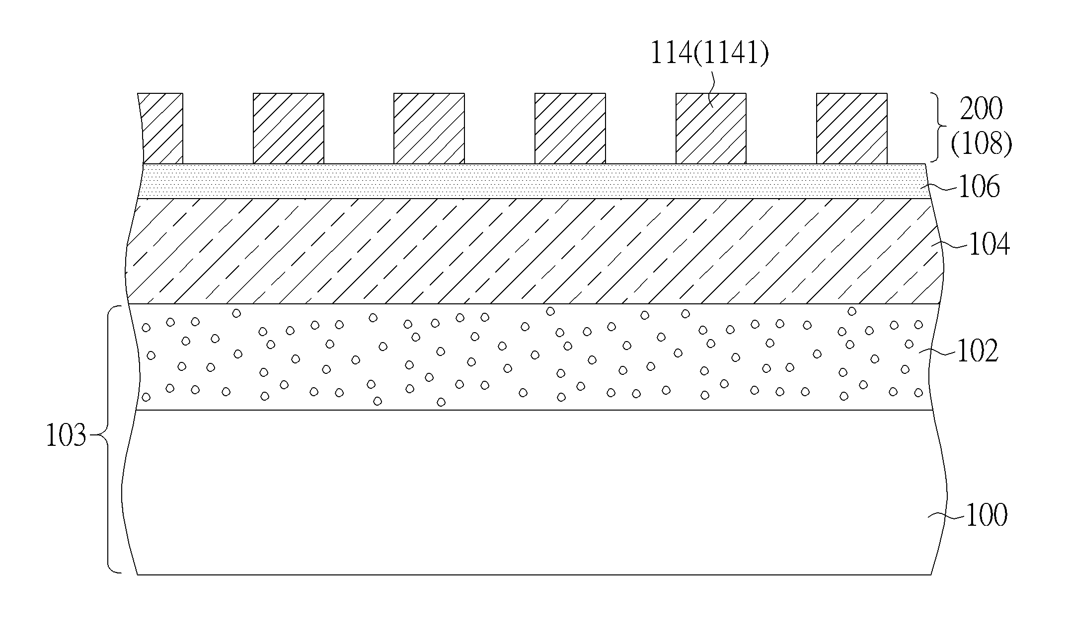
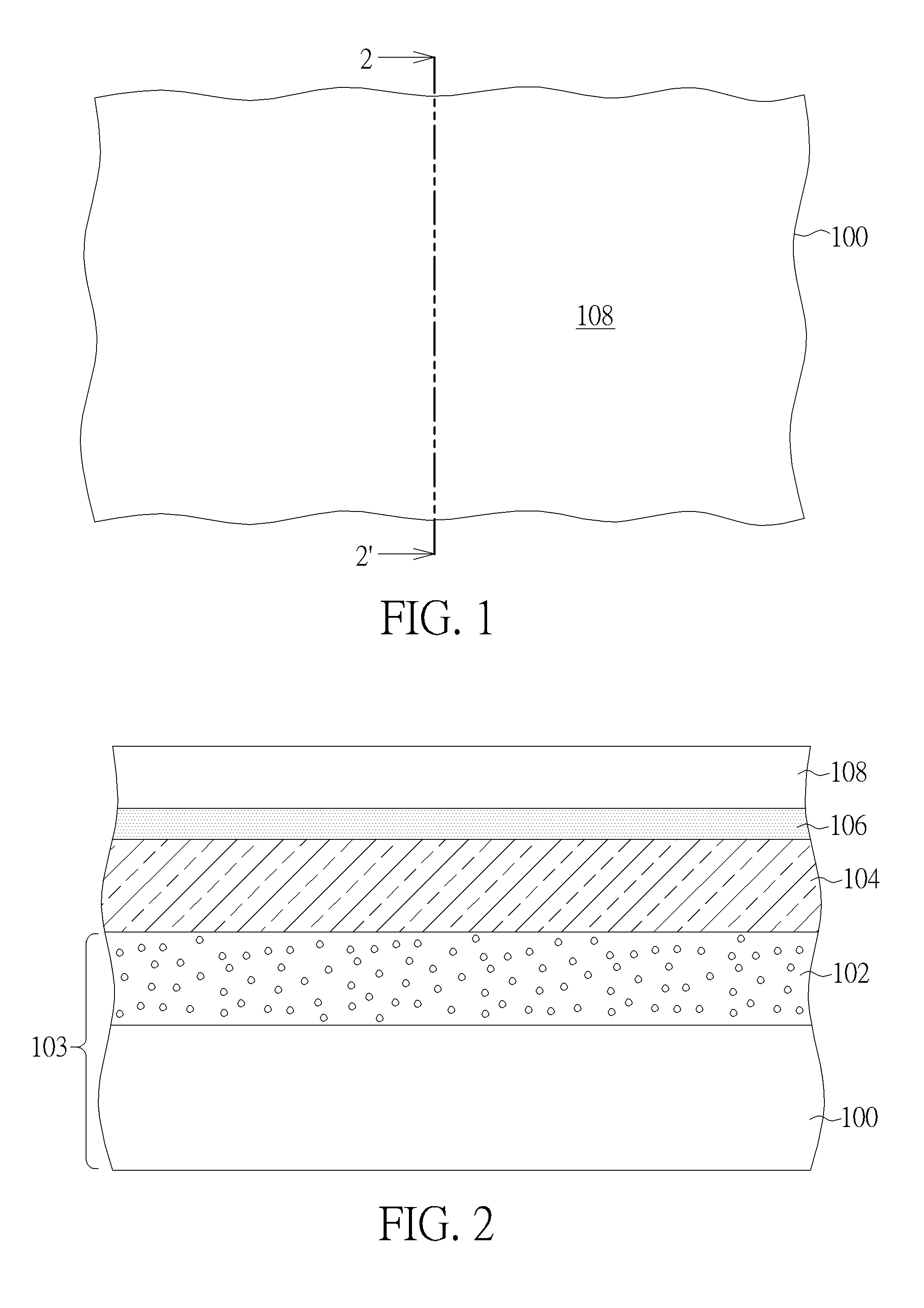
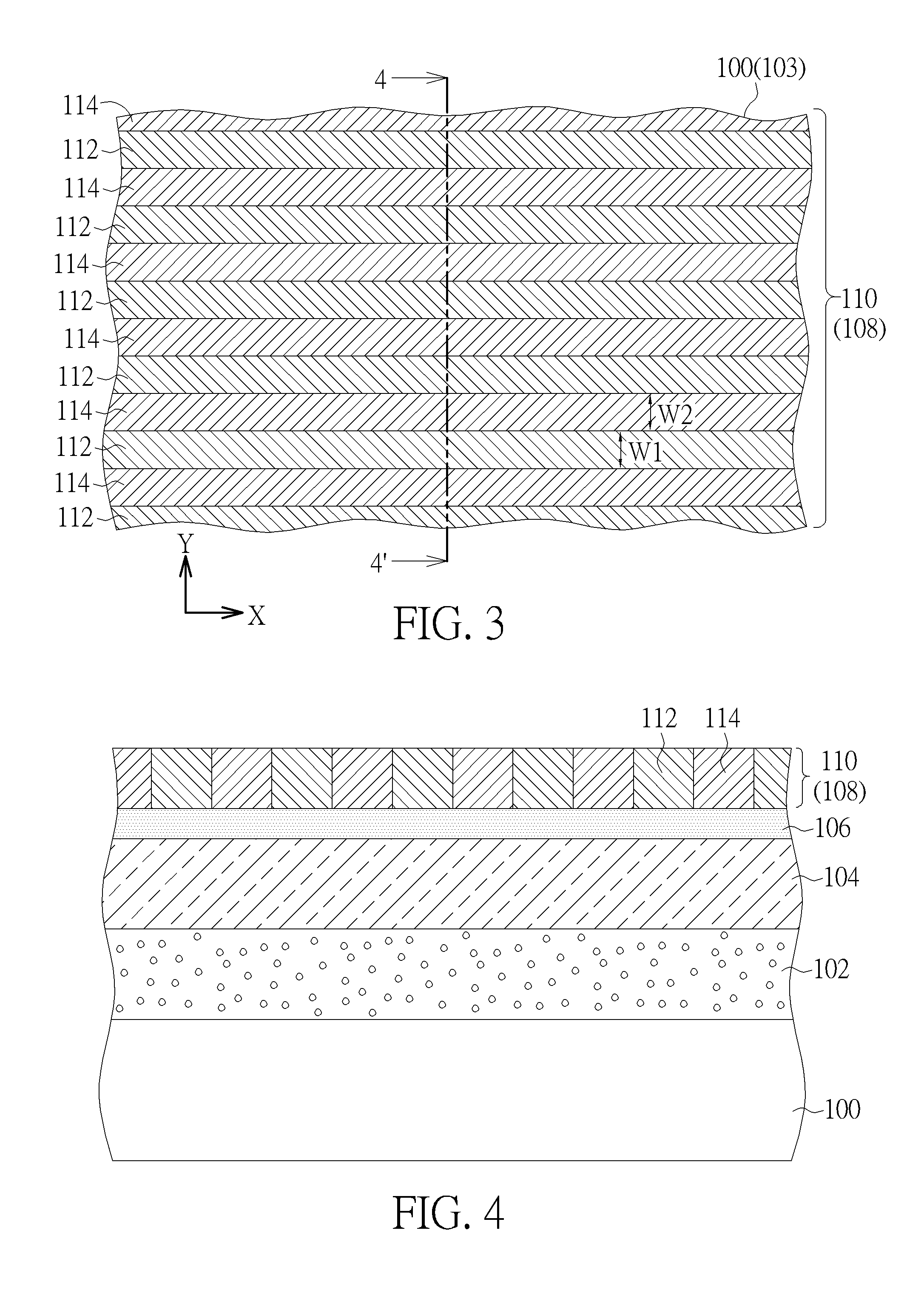
[0024]Please refer to FIG. 1 to FIG. 13. FIG. 1 to FIG. 13 are schematic diagrams of fabrication process of the method of forming a non-continuous line pattern according to an embodiment of the present invention, wherein FIG. 9 illustrates a non-continuous line pattern structure on a semiconductor IC substrate. As shown in FIG. 1 and FIG. 2, FIG. 1 illustrates a schematic diagram of the top view of a semiconductor IC substrate and the material layer disposed thereon, and FIG. 2 is a schematic diagram of the sectional view of the semiconductor IC substrate along the sectional line 2-2′ shown in FIG. 1. According to this embodiment, on...


PUM


Abstract

A method of forming a non-continuous line pattern includes forming a DSA material layer on a substrate, performing a phase separation of the DSA material layer to form an ordered periodic pattern including a plurality of first polymer structures and the second polymer structures arranged alternately, forming a first mask to cover a first portion of the ordered periodic pattern, performing a first etching process to remove a portion of the first polymer structures exposed by the first mask, removing the first mask, forming a second mask to cover a second portion of the ordered periodic pattern, with an interval to the first portion of the ordered periodic pattern, performing a second etching process to remove a portion of the second polymer structures exposed by the second mask, and removing the second mask. The remaining first polymer structures and the remaining second polymer structures are not connected to each other.

Description

BACKGROUND OF THE INVENTION[0001]1. Field of the Invention[0002]The present invention relates to a method of forming non-continuous line pattern and a non-continuous line pattern structure on semiconductor integrated circuit (IC) substrate, and more particularly, to a method of forming non-continuous line pattern and a non-continuous line pattern structure on semiconductor IC substrate by using directed self-assembly (DSA) material.[0003]2. Description of the Prior Art[0004]In recent years, as the continuous decrease of the sizes of semiconductor devices and the increase of the stacking and integration density of semiconductor devices, the photolithography process approaches physical limitation such that the costs of design, process development, and photomask rise dramatically. Therefore, many traditional process tool and fabrication method cannot meet the fabrication requirement anymore. As a result, the manufacturer has to keep on developing more delicate and more expensive tools ...

Claims


Application Information

Patent Timeline
IPC IPC(8): H01L21/027H01L21/311
CPCH01L21/0271H01L21/31127H01L21/31144H01L21/0274H01L29/0657H01L21/0334H01L21/32139H01L21/0275H01L21/0332H01L21/0337H01L21/76816
Inventor CHEN, YU-TELIOU, EN-CHIUANTSENG, CHIA-HSUNSU, SHIN-FENGHUNG, YU-TINGTSAI, MENG-LIN
Owner UNITED MICROELECTRONICS CORP
Why Eureka
Try Eureka