Eureka AIR delivers breakthrough ideas for toughest innovation challenges, trusted by R&D personnel around the world.

Method for reusing and verifying electronic circuits

Active Publication Date: 2016-12-22
CELESTICA TECH CONSULTANCY SHANGHAI
View PDF2 Cites 1 Cited by
  • Summary
  • Abstract
  • Description
  • Claims
  • Application Information

AI Technical Summary

Benefits of technology

The present invention provides a method for reusing and verifying electronic circuits. This helps to correctly reuse the previous circuit design in a new circuit design, reducing development time and production costs. The method utilizes the fingerprints of connections of electronic components to ensure the proper functionality of the circuits.

Problems solved by technology

Manually checking that the reused portion of the previous electronic design has been correctly copied is laborious, and will often miss errors.

Method used


Image

  • Method for reusing and verifying electronic circuits
  • Method for reusing and verifying electronic circuits
  • Method for reusing and verifying electronic circuits

Examples


Embodiment Construction

[0035]The accompanying drawings are included to provide a further understanding of the invention, and are incorporated in and constitute a part of this specification. The drawings illustrate preferred exemplary embodiments of the invention and, together with the description, serve to explain the principles of the invention.

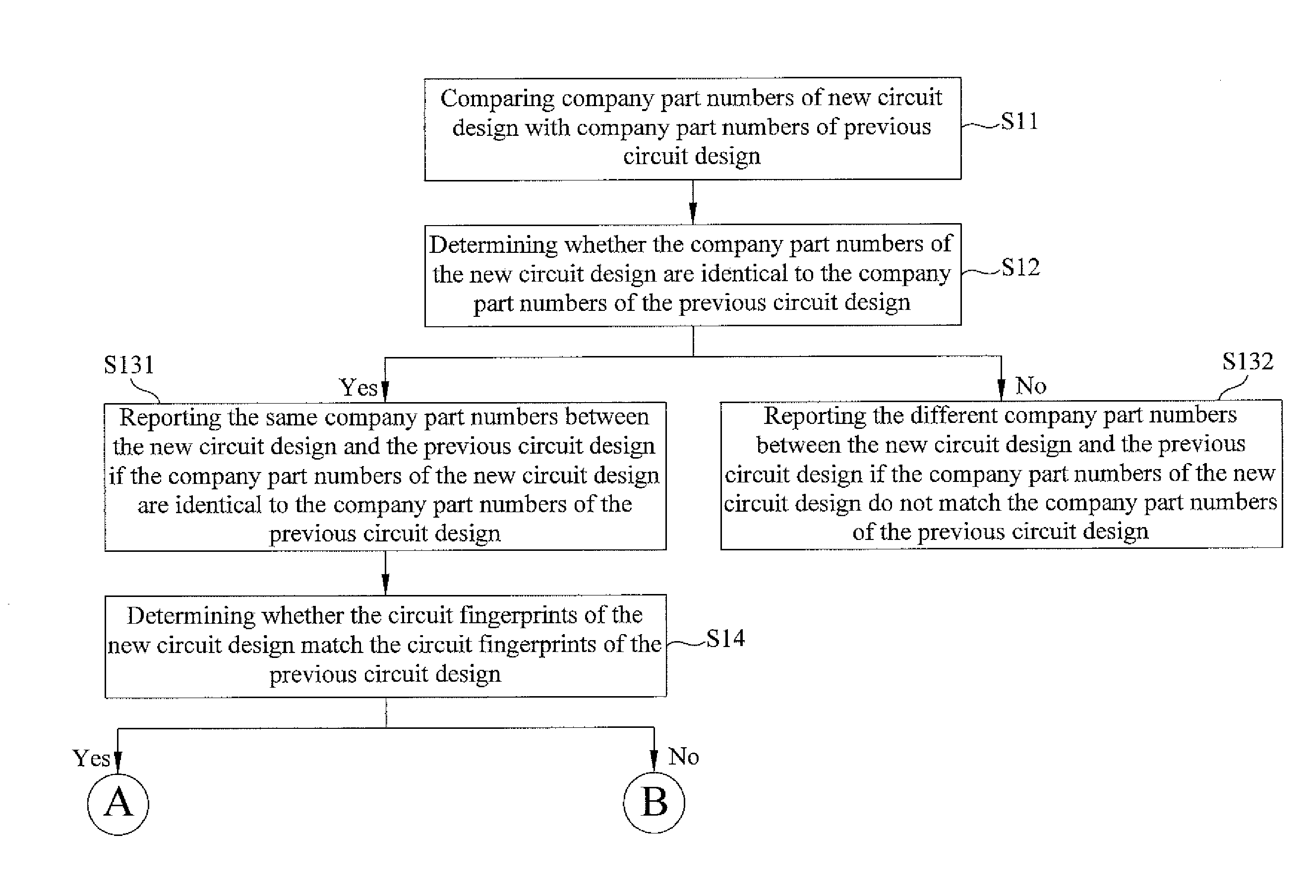
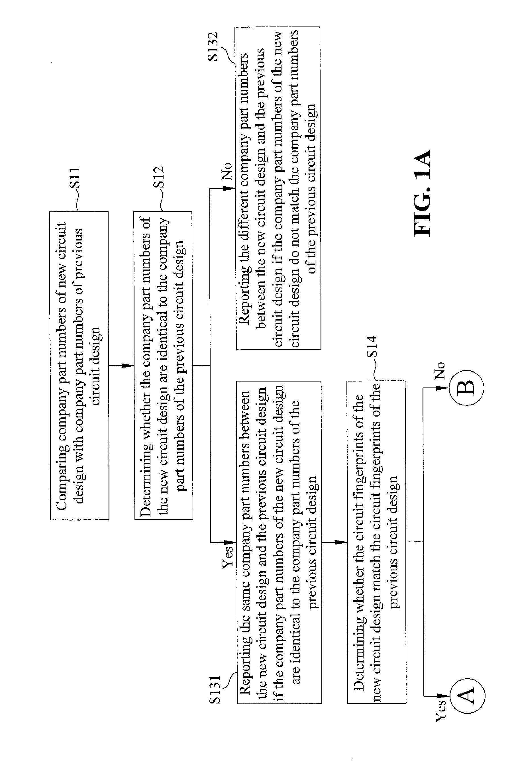
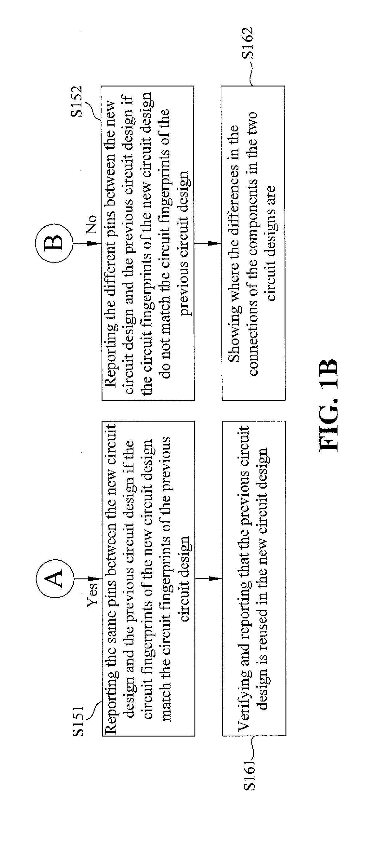
[0036]In light of the foregoing drawings, an objective of the present invention is to provide a method for reusing and verifying electronic circuits. The method for reusing and verifying electronic circuits includes the following steps, as shown in FIGS. 1A and 1B.

[0037]FIGS. 1A and 1B are a flow chart illustrating a method for reusing and verifying electronic circuits by using circuit fingerprints according to the preferred exemplary embodiment of the present invention. As shown in FIG. 1A, the method begins with step S11 of comparing company part numbers of new circuit design with company part numbers of previous circuit design. According to the preferred exempl...


PUM


Abstract

The present invention provides a method for reusing and verifying electronic circuits, including the following steps of comparing company part numbers of new circuit design with company part numbers of previous circuit design; determining whether the company part numbers of the new circuit design are identical to the company part numbers of the previous circuit design; reporting the same company part numbers between the new circuit design and the previous circuit if the company part numbers of the new circuit design are identical to the company part numbers of the previous circuit design; determining whether the circuit fingerprints of the new circuit design match the circuit fingerprints of the previous circuit design; and verifying and reporting that the previous circuit design is reused in the new circuit design if the circuit fingerprints of the new circuit design match the circuit fingerprints of the previous circuit design.

Description

BACKGROUND OF THE INVENTION1. Field of the Invention[0001]The present invention relates to an electronic circuit design, and more particularly, to a method for verifying that portions of a previous electronic design are reused in a new electronic design.2. The Prior Arts[0002]With the rapid development of semiconductor technology and electronic circuit design techniques, a number of different and complex printed circuit boards (PCBs) have been designed in industry. PCBs include the placement of electronic components, such as resistors, capacitors, transistors and the metallic interconnect of these components laminated onto a non-conductive substrate, via conductive traces, pads and other features.[0003]In response to the complex electronic circuit design and the design time requirement, Electronic Design Automation (EDA) software and Electrical Computer Aided Design (ECAD) software are widely used in the design, testing and verification of PCBs.[0004]Each of the components includes ...

Claims


Application Information

Patent Timeline
IPC IPC(8): G06F17/50
CPCG06F17/5081G06F30/30G06F30/3323
Inventor KUNGSAKAWIN, SIRICHAISIRIPORNPERMSAK, RUNGROT
Owner CELESTICA TECH CONSULTANCY SHANGHAI
Why Eureka
Eureka Blog
Learn More