Light-emitting device and method of manufacturing same

a technology of light-emitting devices and manufacturing methods, which is applied in the manufacture of semiconductor/solid-state devices, semiconductor devices, electrical devices, etc., to achieve the effect of improving the optical output of the light-emitting device and suppressing the light absorption by the substra

Active Publication Date: 2016-12-29
NICHIA CORP
View PDF4 Cites 8 Cited by
  • Summary
  • Abstract
  • Description
  • Claims
  • Application Information

AI Technical Summary

Benefits of technology

The present invention helps improve the optical output of a light-emitting device by suppressing the absorption of light by the substrate.

Problems solved by technology

However, the conventional light-emitting device described above may lead to the transparent member (the adhesive) sometimes dripping from between the light-emitting element and the plate-like optical layer (the second light-transmissive member) and reaching an upper surface of a substrate before the transparent member (the adhesive) hardens, thereby causing light emitted from the light-emitting element to travel through the transparent member (the adhesive) and enter the upper surface of the substrate to be absorbed by the substrate.

Method used


Image

  • Light-emitting device and method of manufacturing same
  • Light-emitting device and method of manufacturing same
  • Light-emitting device and method of manufacturing same

Examples


first embodiment

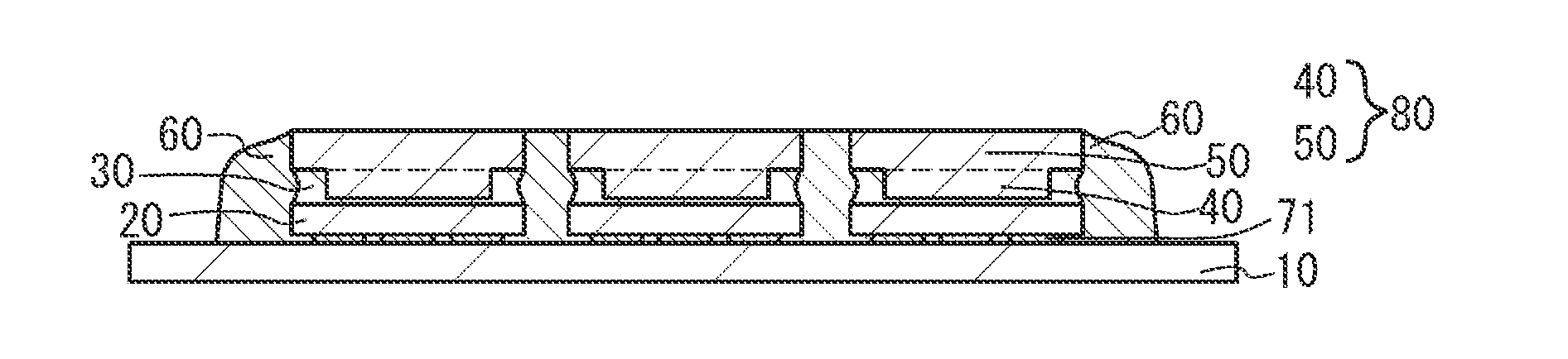
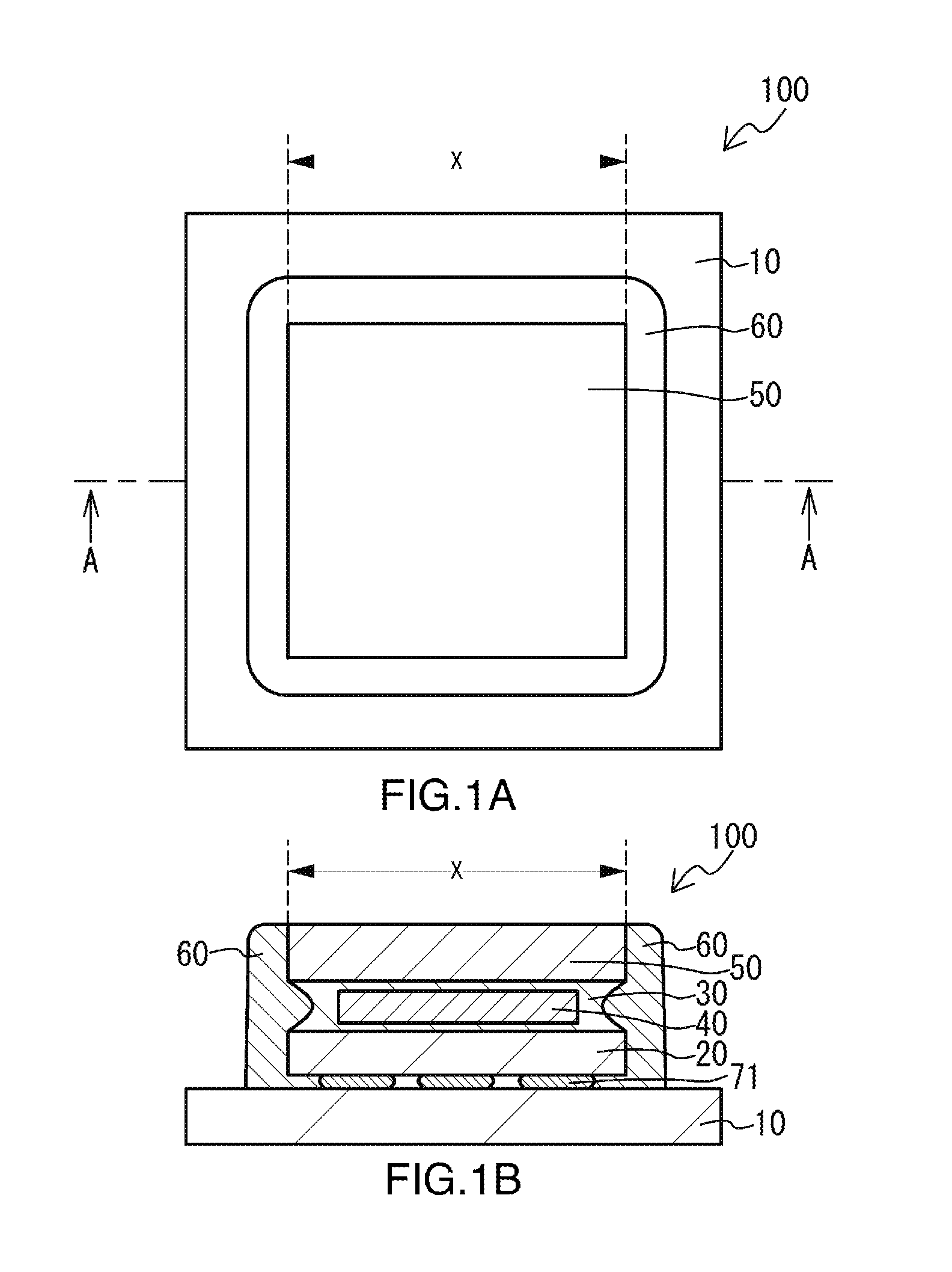
[0017][Light-Emitting Device 100 ]

[0018]FIG. 1A is a schematic plan view of a light-emitting device according to a first embodiment and FIG. 1B is a diagram showing a section A-A in FIG. 1A.

[0019]As shown in FIGS. 1A and 1B, a light-emitting device 100 according to the first embodiment includes a substrate 10, a light-emitting element 20 mounted on the substrate 10, a first light-transmissive member 40 bonded to an upper surface of the light-emitting element 20 via an adhesive 30, and a second light-transmissive member 50 placed on an upper surface of the first light-transmissive member 40. A peripheral edge of a lower surface of the first light-transmissive member 40 is positioned more inward than a peripheral edge of the upper surface of the light-emitting element 20 in a plan view, and the adhesive 30 is provided so as to extend from the upper surface of the light-emitting element 20 to a lower surface of the second light-transmissive member 50 while covering a side surface of th...

second embodiment

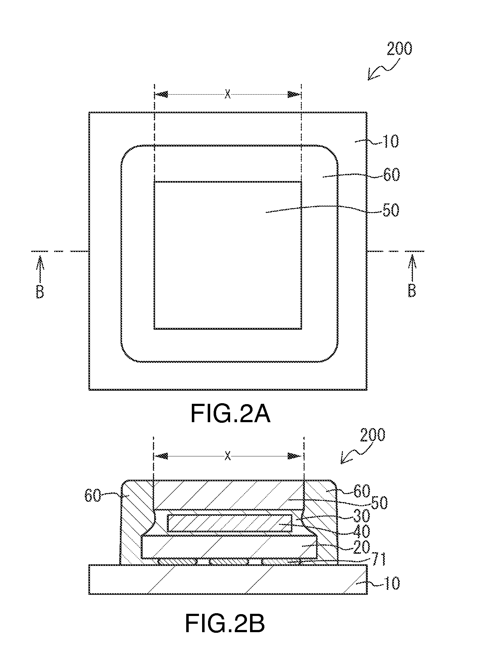
[0051][Light-Emitting Device 200 ]

[0052]FIG. 2A is a schematic plan view of a light-emitting device according to a second embodiment and FIG. 2B is a diagram showing a section B-B in FIG. 2A.

[0053]As shown in FIGS. 2A and 2B, the light-emitting device 200 according to the second embodiment is a light-emitting device in which the peripheral edge of the lower surface of the second light-transmissive member 50 is positioned more inward than the peripheral edge of the upper surface of the light-emitting element 20 in a plan view, while the light-emitting device 100 according to the first embodiment is a light-emitting device in which the lower surface of the second light-transmissive member 50 has a same shape as the light-emitting element 20 in a plan view. With the light-emitting device 200 according to the second embodiment, absorption of light by the substrate 10 can be suppressed and optical output of the light-emitting device can be improved in a similar manner to the light-emitti...

third embodiment

[0058][Light-Emitting Device 300 ]

[0059]FIG. 3A is a schematic plan view of a light-emitting device according to a third embodiment and FIG. 3B is a diagram showing a section C-C in FIG. 3A.

[0060]As shown in FIGS. 3A and 3B, the light-emitting device 300 according to the third embodiment is a light-emitting device in which the peripheral edge of the lower surface of the second light-transmissive member 50 is positioned more outward than the peripheral edge of the upper surface of the light-emitting element 20 in a plan view, while the light-emitting device 100 according to the first embodiment is a light-emitting device in which the lower surface of the second light-transmissive member 50 has a same shape as the light-emitting element 20 in a plan view. With the light-emitting device 300 according to the third embodiment, absorption of light by the substrate 10 can be suppressed and optical output of the light-emitting device can be improved as well as the light-emitting device 100 ...


PUM


Abstract

A light-emitting device includes a substrate; a light-emitting element mounted on the substrate; a first light-transmissive member bonded to an upper surface of the light-emitting element via an adhesive; and a second light-transmissive member placed on an upper surface of the first light-transmissive member. In a plan view of the light-emitting device, a peripheral edge of a lower surface of the first light-transmissive member is positioned more inward than a peripheral edge of the upper surface of the light-emitting element. The adhesive extends from the upper surface of the light-emitting element to a lower surface of the second light-transmissive member, the adhesive covers a side surface of the first light-transmissive member, and the adhesive is separated from the substrate.

Description

CROSS-REFERENCE TO RELATED APPLICATIONS[0001]The present application is a divisional of U.S. patent application Ser. No. 14 / 657,913, filed on Mar. 13, 2015, which claims priority to Japanese Patent Application No. 2014-051754, filed on Mar. 14, 2014, and Japanese Patent Application No. 2015-035340, filed on Feb. 25, 2015, the contents of which are all hereby incorporated by reference in their entireties.BACKGROUND1. Field[0002]The present disclosure relates to a light-emitting device and a method of manufacturing the light-emitting device.2. Description of the Related Art[0003]Conventionally, a light-emitting device has been proposed in which a plate-like optical layer (a second light-transmissive member) is bonded to a light-emitting element via a transparent member (an adhesive) (refer to Japanese Patent Application Laid-open No. 2012-4303).[0004]However, the conventional light-emitting device described above may lead to the transparent member (the adhesive) sometimes dripping fro...

Claims


Application Information

Patent Timeline
Patent Type & Authority Applications(United States)
IPC IPC(8): H01L33/54H01L33/60H01L33/56H01L27/15H01L33/50
CPCH01L33/54H01L27/15H01L33/502H01L2933/0058H01L33/60H01L2933/0041H01L2933/005H01L33/56H01L33/505H01L33/507H01L2924/181H01L2224/73253H01L25/0753H01L33/52H01L33/58H01L2924/00012H01L27/156
Inventor MIYOSHI, TOMONORIOZEKI, KENJI
Owner NICHIA CORP
Why Eureka
Try Eureka