Method for fabricating capacitor

Active Publication Date: 2017-01-05
ASUSTEK COMPUTER INC
View PDF1 Cites 0 Cited by
  • Summary
  • Abstract
  • Description
  • Claims
  • Application Information

AI Technical Summary

Benefits of technology

[0007]In sum, according to the method for fabricating the capacitor, the dielectric layer is formed by a chemical vapor deposition such as an atomic layer deposition process which results in thin and uniform thickness. Thus, the capacitor is thin in size and has a quick charge characteristic. Furthermore, in embodiments, since the first inner electrodes and the second inner electr

Problems solved by technology

However, the volume of a common MLCC or SC is large.
In addition, the MLCC or SC cannot be used at a low environmental

Method used


Image

  • Method for fabricating capacitor
  • Method for fabricating capacitor
  • Method for fabricating capacitor

Examples


Example

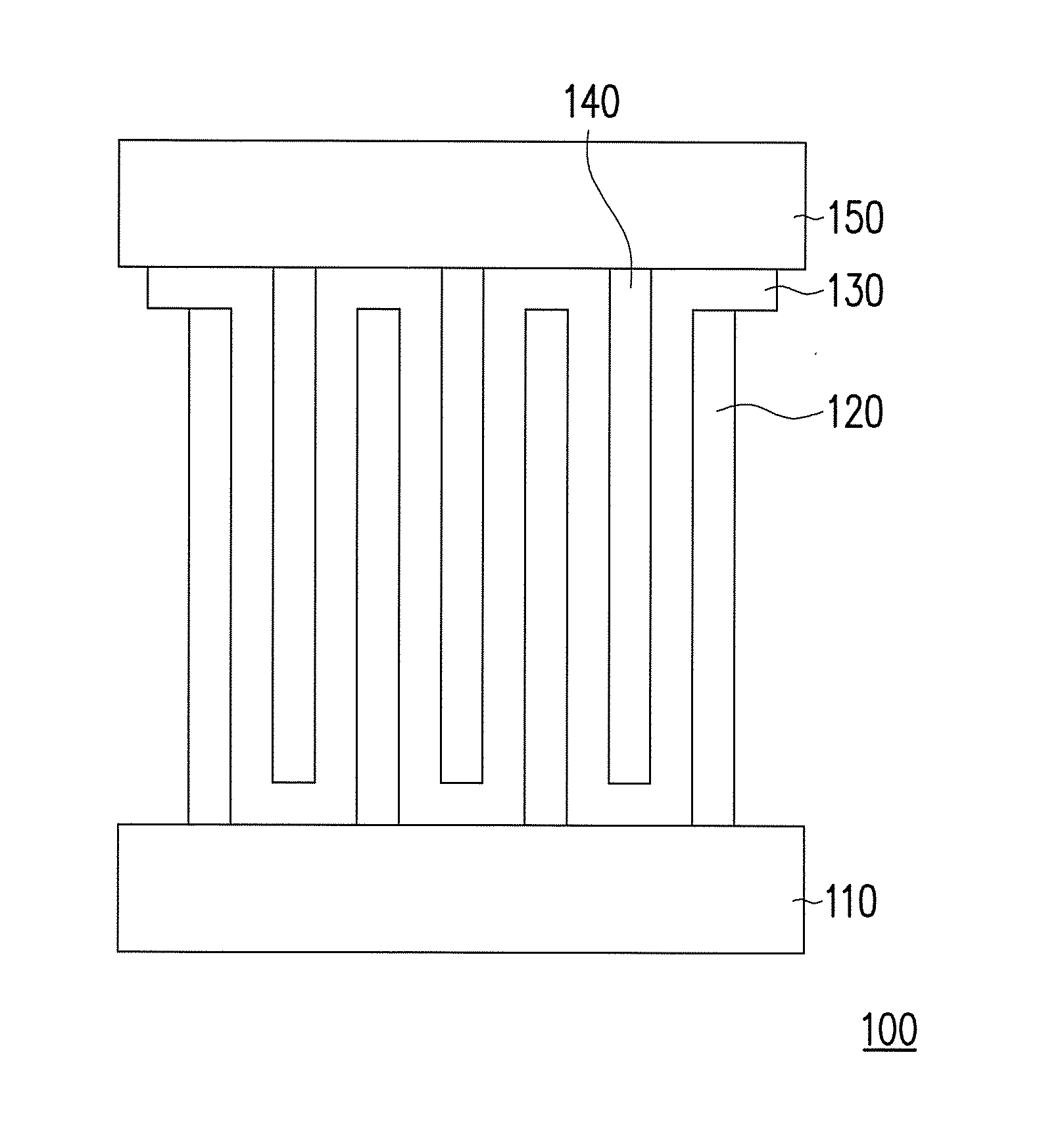
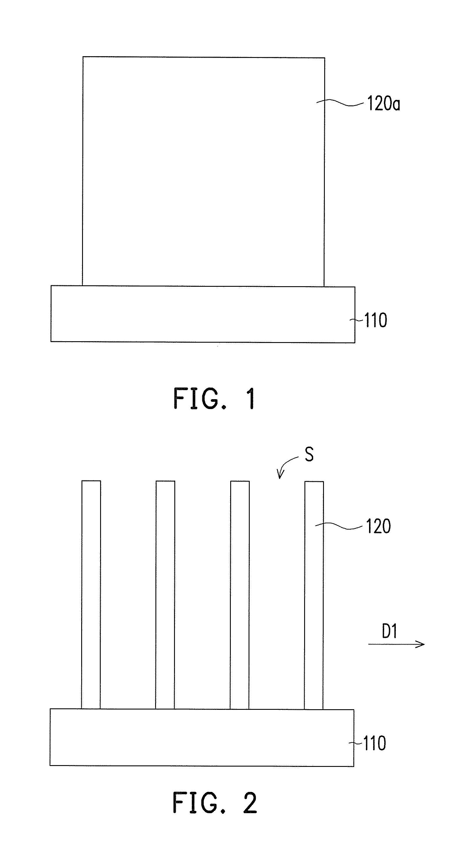
[0010]FIG. 1 to FIG. 5 are section views of intermediate structures in manufacturing a capacitor in an embodiment. Referring to FIG. 1, a substrate 110 and a first conducting material layer 120a are provided. The first conducting material layer 120a is formed on the substrate 110. In the embodiment, the substrate 110 is formed of metal (such as, copper, silver and aluminum), and the substrate 110 is used as the first external electrode. In the embodiment, the first conducting material layer 120a is formed of nitride (such as TiN, TaN and CuN), metal (such as copper, platinum, silver, ruthenium and nickel) or other suitable materials, which is not limited herein.

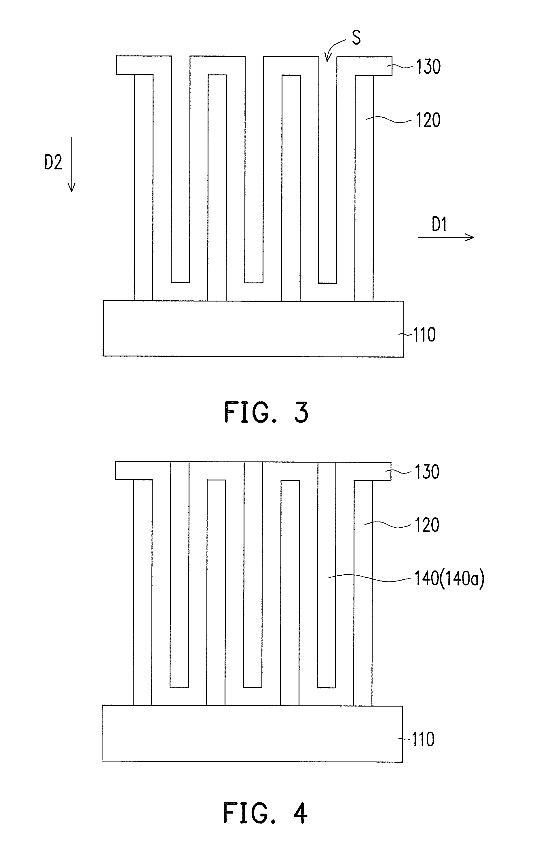
[0011]Retelling to FIG. 2, the substrate 110 is partly exposed by removing a part of the first conducting material layer 120a to form a plurality of first inner electrodes 120. The first inner electrodes 120 are arranged along a first direction D 1. Each of the adjacent first inner electrodes 120 have an interval S therebetwe...


PUM

PropertyMeasurementUnit
Thicknessaaaaaaaaaa
Thicknessaaaaaaaaaa
Electrical conductoraaaaaaaaaa

Abstract

A method for fabricating a capacitor includes following steps: providing a substrate and a first conducting material layer which is disposed on the substrate; removing a part of the first conducting material layer to expose a part of the substrate to form a plurality of first inner electrodes, wherein the first inner electrodes are arranged along a first direction, and the adjacent first inner electrodes have an interval therebetween; forming a dielectric layer along a second direction by a chemical vapor deposition process, wherein the first direction is perpendicular to the second direction so that the dielectric layer covers the first inner electrodes and the exposed part of the substrate, and the dielectric layer does not fully fill the intervals; and forming a second conducting material layer to fill the intervals that are not fully filled by the dielectric layer to form a plurality of second inner electrodes.

Description

CROSS-REFERENCE TO RELATED APPLICATION[0001]This application claims the priority benefit of China application serial No. 201510386903.2, filed on Jul. 3, 2015. The entirety of the above-mentioned patent application is hereby incorporated by reference herein and made a part of this specification.BACKGROUND OF THE INVENTION[0002]Field of the Invention[0003]The invention relates to a method for fabricating a semiconductor element and, more specifically, to a method for fabricating a capacitor.[0004]Description of the Related Art[0005]Conventionally, a multi-layer ceramic capacitor (MLCC) or a super capacitor (SC) (which is also called as electrical double layer capacitor (EDLC)) is used, for example, as an input capacitor, in a power supply circuit of a central processing unit (CPU) in a personal computer or a notebook to reduce the cost and the volume of the element. However, the volume of a common MLCC or SC is large. And also, the MLCC or SC only can be used under a limited environm...

Claims


Application Information

Patent Timeline
IPC IPC(8): H01L49/02
CPCH01L28/92H01G4/12H01G4/33H01L28/55
Inventor LIN, BIN-YI
Owner ASUSTEK COMPUTER INC
Why Eureka
Try Eureka