

Structure containing self-aligned conductive lines and fabricating method thereof
- Summary
- Abstract
- Description
- Claims
- Application Information
AI Technical Summary
Benefits of technology
Problems solved by technology
Method used
Image

Examples
first embodiment
The First Embodiment
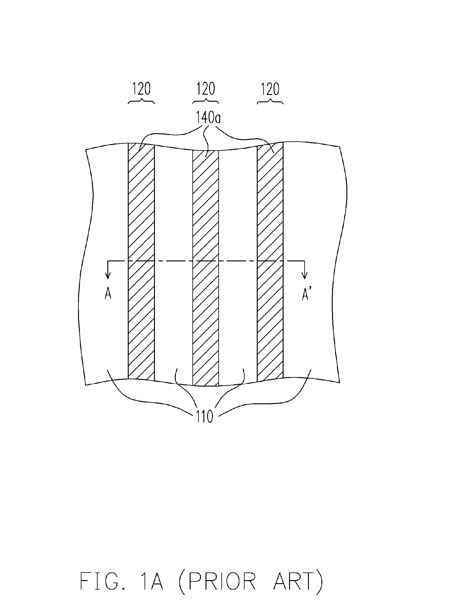
[0038]FIGS. 2A-2C are schematic cross-sectional views of a process of fabricating self-aligned conductive lines along line A-A′ in FIG. 1A in an embodiment of the present invention. Please refer to FIGS. 2A-2C.
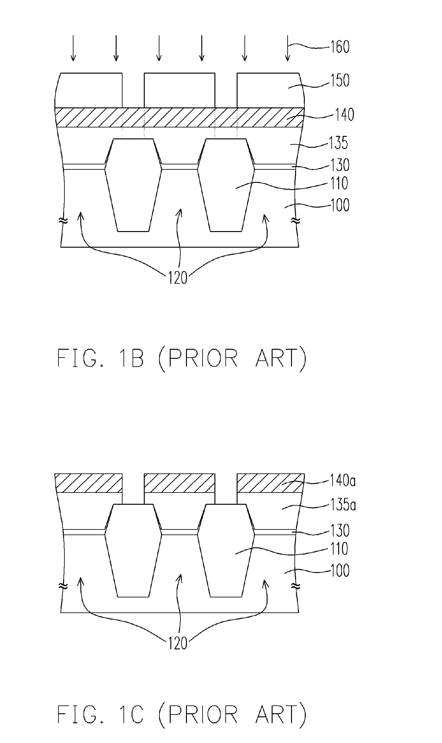
[0039] Referring to FIG. 2A, first the substrate 200 is provided. A plurality of isolation structures 210 previously formed in the substrate 200 are protrusive from the surface of substrate 200. An active region 220 is defined between the adjacent isolation structures 210. In the active region 220, a plurality of devices have been formed previously (not shown). The isolation structures 210 are much higher than the devices. In an embodiment, the isolation structures 210 are in bar layout, and the fabricating method thereof is, for example, shallow trench isolation (STI) process. The active region 220 is defined between the isolation structures 210 in bar layout. In the active region 220, a plurality of semiconductor devices are trench devices, for example (...
second embodiment
The Second Embodiment
[0049]FIG. 3A is a schematic top view of an array containing trench devices. FIG. 3B is a schematic cross-sectional view showing a process of fabricating the word line along line B-B′ in the process for fabricating an array containing trench devices. Please refer to FIGS. 3A and 3B.
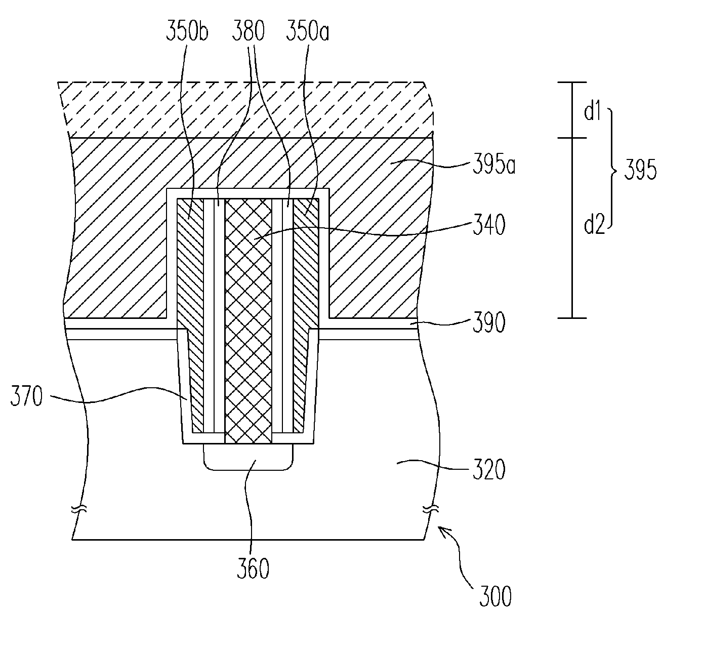
[0050] As shown in FIGS. 3A and 3B, the substrate 320 is provided. A plurality of isolation structures 310 previously formed in the substrate 320 are protrusive from the surface of the substrate 320. Furthermore, an active region 330 is defined between the adjacent isolation structures 310. In the active region 330, a plurality of trench devices 300 have been formed previously. The method for forming the trench devices 300 is apparent to those skilled in the art, and is omitted in the specification.
[0051] Referring to FIG. 3B, in an embodiment of the present invention, the trench device 300 is, for example, a trench flash memory cell, and the trench device 300 includes at least a tu...
PUM
 Abstract
Description
Claims
Application Information