

Amoled pixel driving circuit and pixel driving method
- Summary
- Abstract
- Description
- Claims
- Application Information
AI Technical Summary
Benefits of technology
Problems solved by technology
Method used
Image

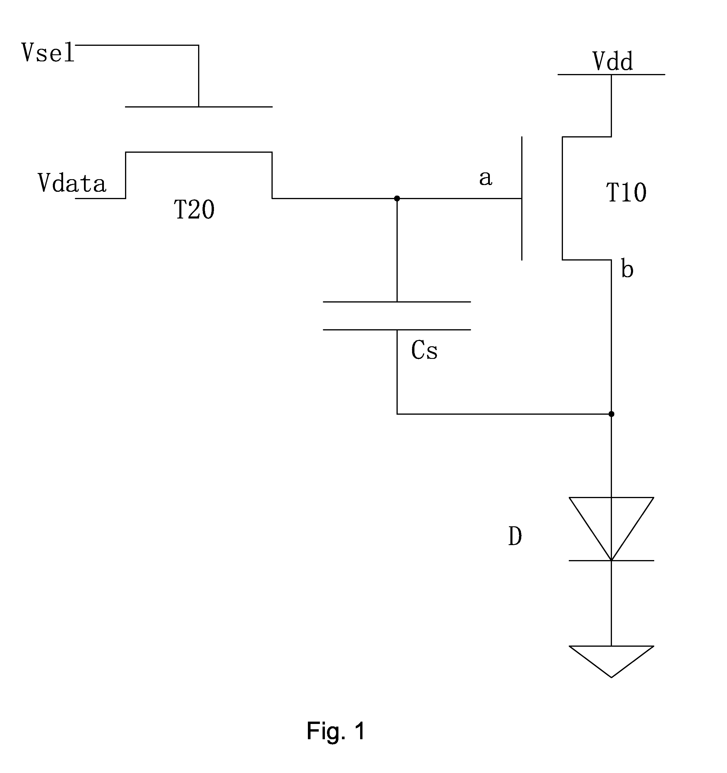
Examples
Embodiment Construction
[0078]For better explaining the technical solution and the effect of the present invention, the present invention will be further described in detail with the accompanying drawings and the specific embodiments.
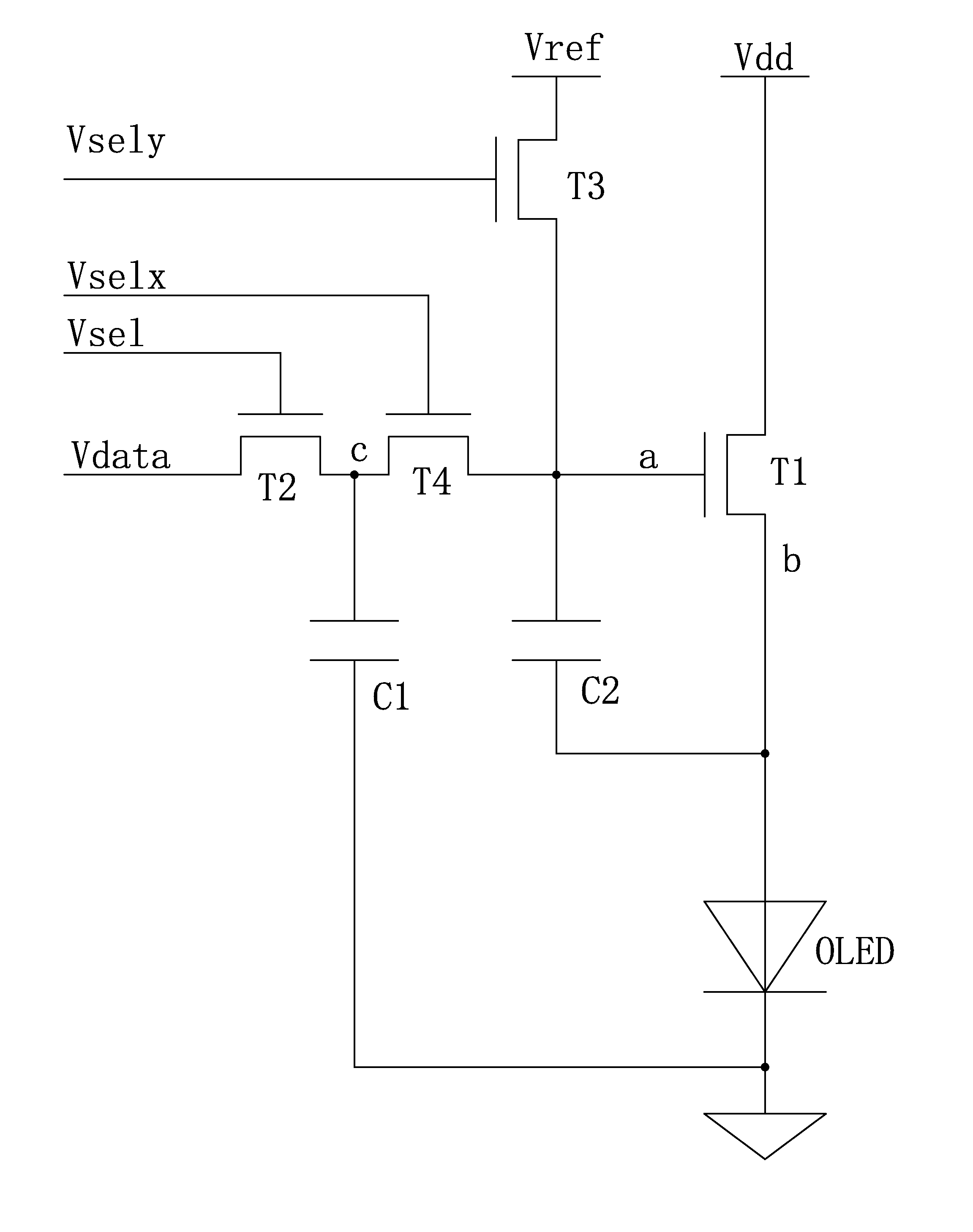
[0079]Please refer to FIG. 3. The present invention first provides an AMOLED pixel driving circuit, and the AMOLED pixel driving circuit comprises: a first thin film transistor T1, a second thin film transistor T2, a third thin film transistor T3, a fourth thin film transistor T4, a first capacitor C1, a second capacitor C2 and an organic light emitting diode OLED.
[0080]a gate of the first transistor T1 is electrically coupled to a first node a, and a source is electrically coupled to a second node b, and a drain is electrically coupled to an alternating current power supply voltage Vdd;
[0081]a gate of the second thin film transistor T2 is electrically coupled to a scan signal voltage Vsel, and a source is electrically coupled to a data signal voltage Vdata, and a drain is ele...
PUM
 Abstract
Description
Claims
Application Information