Touch display device and manufacturing method thereof

a technology of touch display and manufacturing method, which is applied in the field of electronic devices, can solve the problems that the conducting wires cannot transmit signals effectively, and achieve the effect of preventing damage to the conducting wires

Inactive Publication Date: 2017-05-11
ACER INC
View PDF11 Cites 21 Cited by
  • Summary
  • Abstract
  • Description
  • Claims
  • Application Information

AI Technical Summary

Benefits of technology

[0008]The invention is directed to a touch display device and a manufacturing method thereof. The touch display device can prevent damage to the conducting wires disposed on the flexible touch display panel when the flexible touch display panel is bent.
[0013]Based on the above, to prevent damage to the conducting wires due to bending, any conducting wire having a direction different from the axial direction of the bending axis is not disposed in the bending area of the flexible touch display panel. Accordingly, in the embodiments of the invention the life of conducting wires disposed in the flexible touch display panel is increased and effective signal transmission in the touch display device is maintained. Moreover, in the embodiments of the invention, the design space of the touch display device is improved by adding functions to the touch display device through coupling designs between the flexible circuit board and the flexible touch display panel, or by adding a sensor in the bending area of the flexible circuit board.

Problems solved by technology

After repeated bending, some of the conducting wires 116 in the bending area 110B1 may break down due to repeated bending, such that the conducting wires can no longer effectively transmit signal.

Method used


Image

  • Touch display device and manufacturing method thereof
  • Touch display device and manufacturing method thereof
  • Touch display device and manufacturing method thereof

Examples


Embodiment Construction

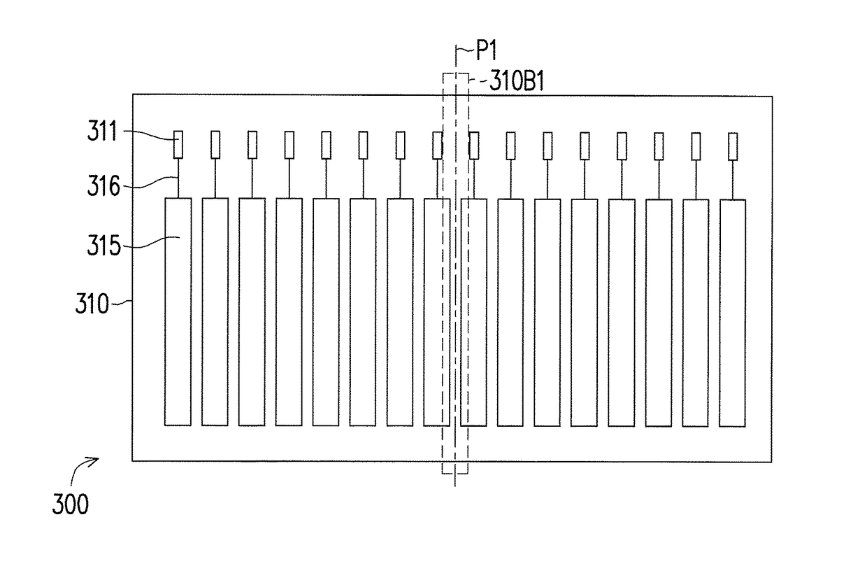
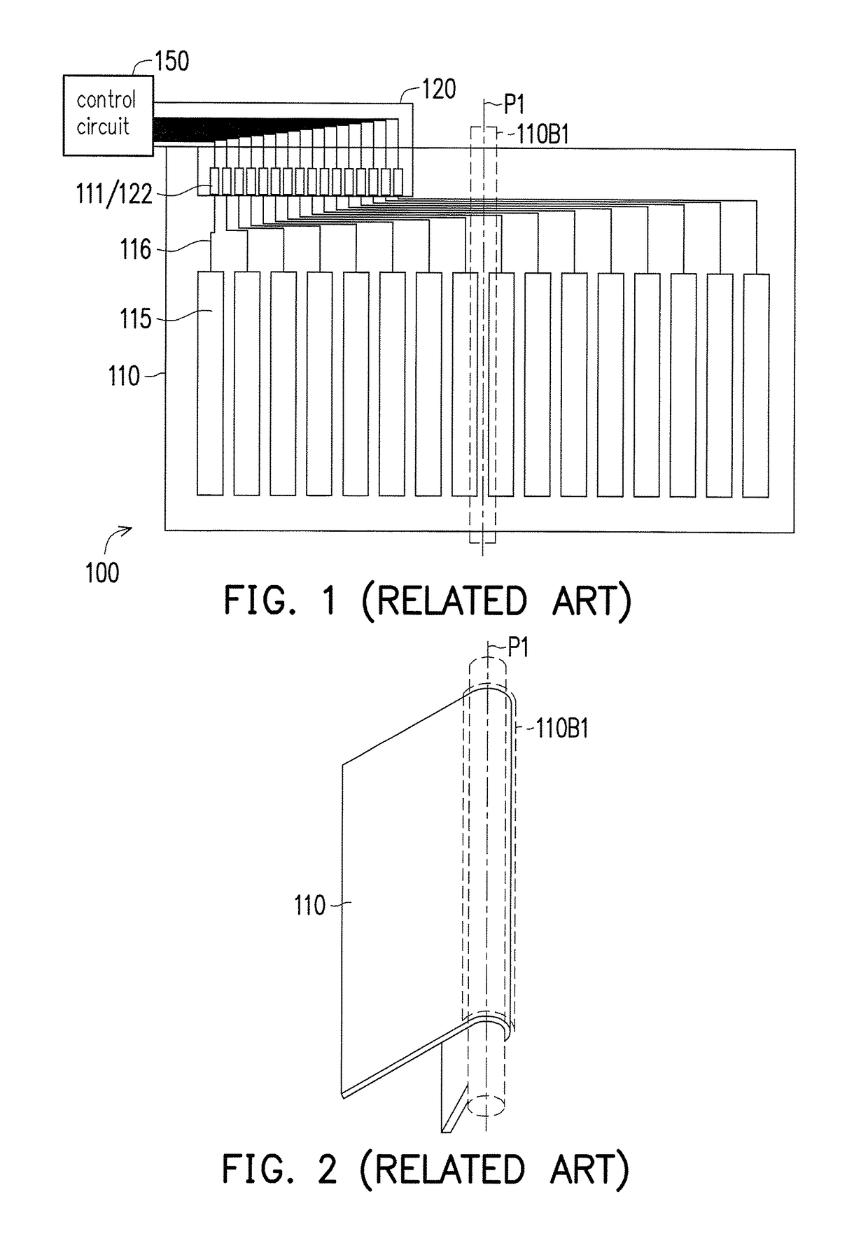
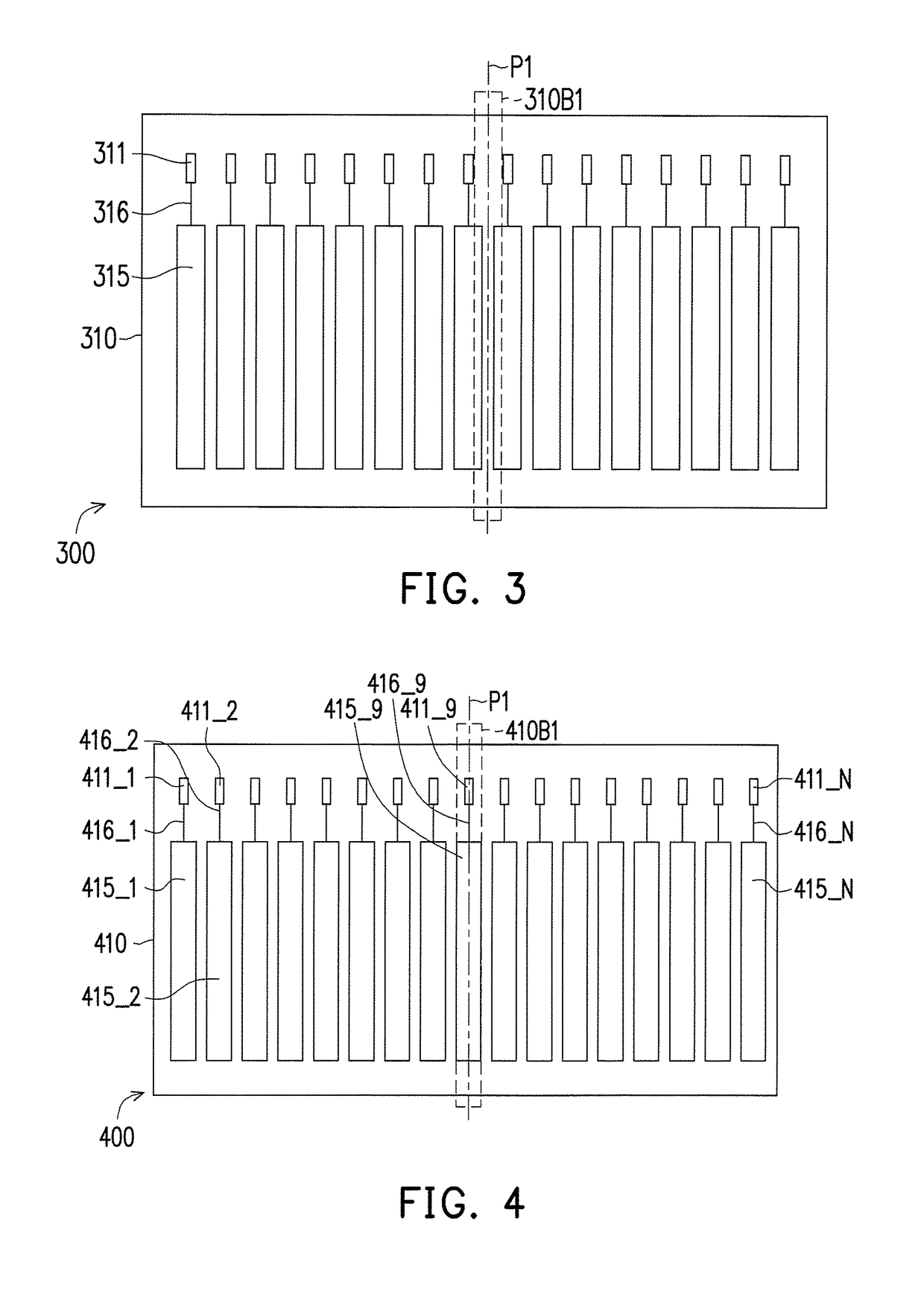
[0032]Reference will now be made in detail to the present preferred embodiments of the invention, instances of which are illustrated in the accompanying drawings. Wherever possible, the same reference numbers are used in the drawings and the description to refer to the same or like parts.

[0033]The word “couple” (or connect) in the description and claims may refer to any direct or indirect connection. For instance, in the description and claims, if first pads are coupled to (or connected to) second pads, it means that the first pads may be directly connected to the second pads or may be indirectly connected to the second pads through another device, wire, or other connection means. Moreover, elements / components / steps with the same reference numerals represent the same or similar parts in the drawings and embodiments. The descriptions of the same elements / components / steps in an embodiment of the invention may be applied to the descriptions of the same elements / components / steps in anot...


PUM


Abstract

A touch display device and a manufacturing method thereof are provided. The touch display device includes a flexible touch display panel, a plurality of first pads, a plurality of touch electrodes and a plurality of conducting wires. The flexible touch display panel includes a first bending area bending along a first bending axis. The first pads are disposed on the flexible touch display. The touch electrodes are disposed on the flexible touch display. The conducting wires are disposed on the flexible touch display. A plurality of first terminals of the conducting wires is electrically coupled to the touch electrodes respectively, and a plurality of second terminals of the conducting wires is electrically coupled to the first pads respectively. Conducting wires having a direction different from the axial direction of the first bending axis are not disposed in the first bending area of the flexible touch display panel.

Description

CROSS-REFERENCE TO RELATED APPLICATION[0001]This application claims the priority benefit of Taiwan application serial no. 104136408, filed on Nov. 5, 2015. The entirety of the above-mentioned patent application is hereby incorporated by reference herein and made a part of this specification.BACKGROUND OF THE INVENTION[0002]Field of the Invention[0003]The invention relates to an electronic device; more particularly, the invention relates to a touch display device and a manufacturing method thereof.[0004]Description of Related Art[0005]Transparent conductive films (e.g. indium tin oxide, abbreviated as ITO) materials can be used in various flexible electronic products such as electronic book flexible mobile phones, flexible displays, disposable electronic products, wearable or mounted products. Flexible electronics technology allows electrical products to be soft and flexible, realizing features such as being lightweight, thin, short, and small, such that they meet the demands of bein...

Claims


Application Information

Patent Timeline
Patent Type & Authority Applications(United States)
IPC IPC(8): G06F3/044G06F1/16
CPCG06F3/044G06F2203/04103G06F2203/04102G06F1/1652G06F3/04164
Inventor LIN, JIA-YUKUO, JIN-TING
Owner ACER INC
Why Eureka
Try Eureka