Antenna device and electronic apparatus

Inactive Publication Date: 2017-07-06
MURATA MFG CO LTD
View PDF6 Cites 8 Cited by
  • Summary
  • Abstract
  • Description
  • Claims
  • Application Information

AI Technical Summary

Benefits of technology

[0020]Preferably, the casing includes a conductor portion, and the conductor portion defines the planar conductor. Thus, because the conductor portion of the casing is also able to provide the planar conductor, it is not necessary to include a special exclusive planar conductor, and size and cost are able to be reduced. In addition, because the planar conductor is located on the outer surface of the electronic apparatus or at a position adjacent to or in a vicinity of the outer surface, the planar con

Problems solved by technology

For this reason, a magnetic field generated by the induced current is also not large, and it is difficult to use the one-turn coil as a radiation element.
For this reason, the structure and formation method of the conductor pat

Method used


Image

  • Antenna device and electronic apparatus
  • Antenna device and electronic apparatus
  • Antenna device and electronic apparatus

Examples


first preferred embodiment

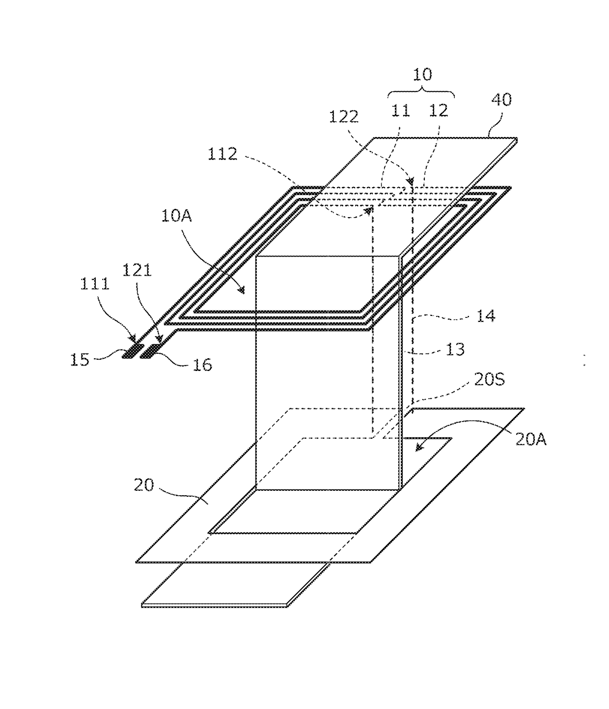
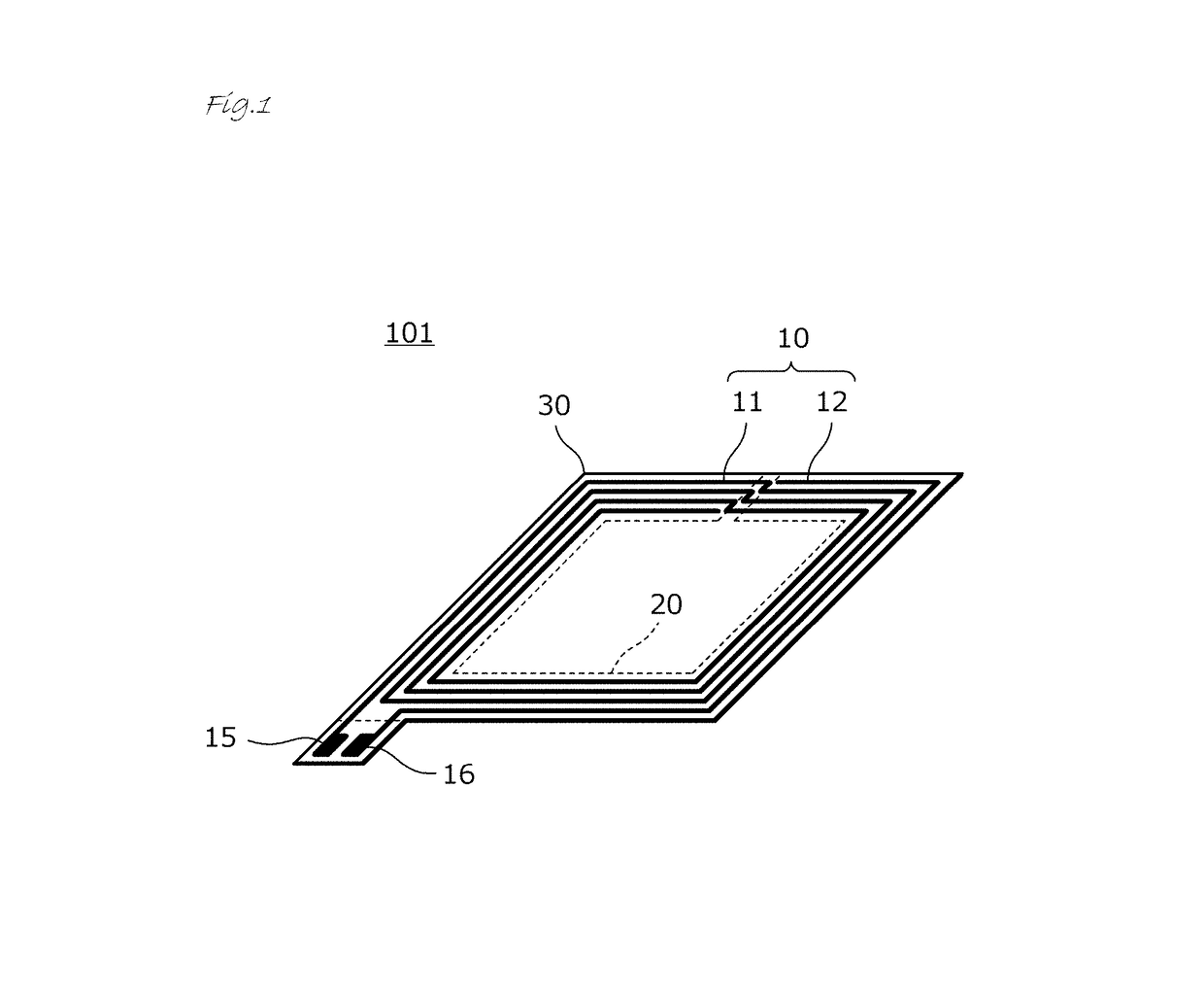
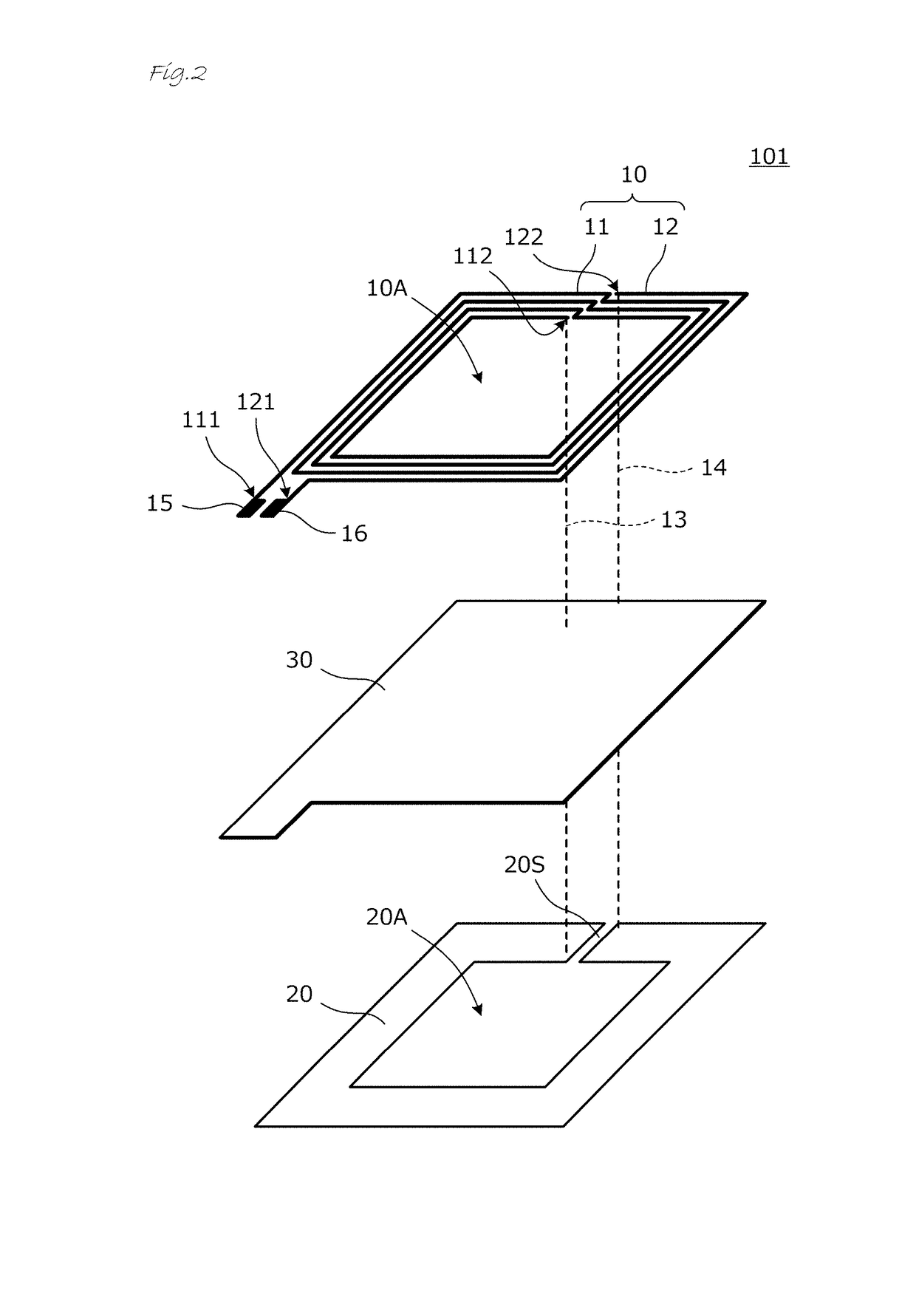
[0042]FIG. 1 is a perspective view of an antenna device 101 according to a first preferred embodiment of the present invention, and FIG. 2 is an exploded perspective view of the antenna device 101.

[0043]The antenna device 101 includes a planar coil 10, a planar conductor 20 opposed to the planar coil 10 with an insulating layer 30 interposed therebetween, a first power feed terminal 15, and a second power feed terminal 16. The planar coil 10 includes a first conductor pattern portion 11 and a second conductor pattern portion 12 wound around a coil aperture 10A along a surface of the insulating layer 30. The planar conductor 20 includes a cutout defined by a conductor aperture 20A overlapping with the coil aperture 10A and a slit 20S that connects a portion of the conductor aperture 20A to an outer edge. The planar conductor 20 is substantially C-shaped in plan view. The first power feed terminal 15 and the second power feed terminal 16 are located in an outer side portion of a regio...

second preferred embodiment

[0057]FIG. 8 is an exploded perspective view of an antenna device 102 according to a second preferred embodiment of the present invention. The antenna device 102 includes a planar coil 10, a planar conductor 20 opposed to the planar coil 10 with an insulating layer 30 interposed therebetween, a first power feed terminal 15, and a second power feed terminal 16. The planar coil 10 includes a first conductor pattern portion 11 and a second conductor pattern portion 12 wound around a coil aperture 10A along a surface of the insulating layer 30. The planar conductor 20 includes a conductor aperture 20A that overlaps with the coil aperture 10A and a slit 20S that connects a portion of the conductor aperture 20A to an outer edge. The first power feed terminal 15 and the second power feed terminal 16 are located in an outer side portion of a region including the conductor pattern portions 11 and 12 in plan view.

[0058]The antenna device 102 of the second preferred embodiment and the antenna ...

third preferred embodiment

[0065]FIG. 10 is an exploded perspective view of an antenna device 103 according to a third preferred embodiment of the present invention. The antenna device 103 includes a planar coil 10, a planar conductor 20 opposed to the planar coil 10 with an insulating layer 30 interposed therebetween, a first power feed terminal 15, and a second power feed terminal 16. The planar coil 10 includes a first conductor pattern portion 11 and a second conductor pattern portion 12 wound around a coil aperture 10A along a surface of the insulating layer 30.

[0066]The antenna device 103 of the third preferred embodiment is different in the structure of the planar coil 10 from the antenna device 101 of the first preferred embodiment and the antenna device 102 of the second preferred embodiment. In the antenna device 103 of the third preferred embodiment, the second conductor pattern portion 12 overlaps with the first conductor pattern portion 11 in plan view.

[0067]Since the first conductor pattern port...


PUM


Abstract

An antenna device includes a planar coil, a planar conductor, a first power feed terminal, and a second power feed terminal. The planar conductor includes a cutout opposed to the planar coil that overlaps with a coil aperture. The planar coil includes a first conductor pattern portion and a second conductor pattern portion. The first power feed terminal is connected to a first end of the first conductor pattern portion and the second power feed terminal is connected to a first end of the second conductor pattern portion on a side adjacent to or in a vicinity of the first end of the first conductor pattern portion. Second ends of the first conductor pattern portion and the second conductor pattern portion are connected to the planar conductor.

Description

CROSS REFERENCE TO RELATED APPLICATIONS[0001]This application claims the benefit of priority to Japanese Patent Application No. 2014-111837 filed on May 30, 2014 and is a Continuation Application of PCT / JP2015 / 065184 filed on May 27, 2015. The entire contents of each application are hereby incorporated by reference.BACKGROUND OF THE INVENTION[0002]1. Field of the Invention[0003]The present invention relates to an antenna device preferably for use in, for example, HF-band communication, and relates to an electronic apparatus including the antenna device.[0004]2. Description of the Related Art[0005]A planar coil antenna has been used as an antenna device for an RFID (radio frequency identifier) or NFC (near field communication). In general, the planar coil antenna includes a base material and a rectangular spiral conductor pattern provided on the base material.[0006]Japanese Unexamined Patent Application Publication No. 11-3411 discloses an antenna device in which the inductance of su...

Claims


Application Information

Patent Timeline
IPC IPC(8): H01Q7/06H01Q1/24H01Q1/22H01Q7/00
CPCH01Q7/06H01Q1/2216H01Q1/242H01Q7/00H01F17/0006H01Q1/2225
Inventor NAKANO, SHINICHI
Owner MURATA MFG CO LTD
Why Eureka
Try Eureka