LED package structure

a technology of led package and packaging, applied in the direction of basic electric elements, electrical apparatus, semiconductor devices, etc., can solve the problems of high material cost and time-consuming manufacturing methods, and achieve the effects of improving performance, reducing cost, and high light reflectivity

Active Publication Date: 2017-07-13
LITE ON OPTO TECH (CHANGZHOU) CO LTD +1
View PDF9 Cites 11 Cited by
  • Summary
  • Abstract
  • Description
  • Claims
  • Application Information

AI Technical Summary

Benefits of technology

[0006]The objective of the present disclosure is to provide a UV LED package structure to solve the technical issues. A high light reflectivity in UV wavebands of the UV LED package structure can be provided by using a silicone molding compound and a filler mixed therewith as a reflective housing, such that the UV LED package structure has a better performance and a lower cost.
[0007]The advantageous effect of the present disclosure is that an inorganic material with a wide energy gap mixed with a silicone molding compound (a resin material) is chosen to be a reflective housing of the LED package structure. Such a choice, compared with using ceramics as a material for the reflective housing, a lower manufacture cost and easy production can be achieved in the present disclosure. In combination with the formulas of the present disclosure, a suitable energy gap of filler may be selected in accordance with a desired wavelength of the UV light of the UV LED chip.

Problems solved by technology

However, the material cost is high and manufacturing method is time-consuming.

Method used


Image

  • LED package structure
  • LED package structure
  • LED package structure

Examples


first embodiment

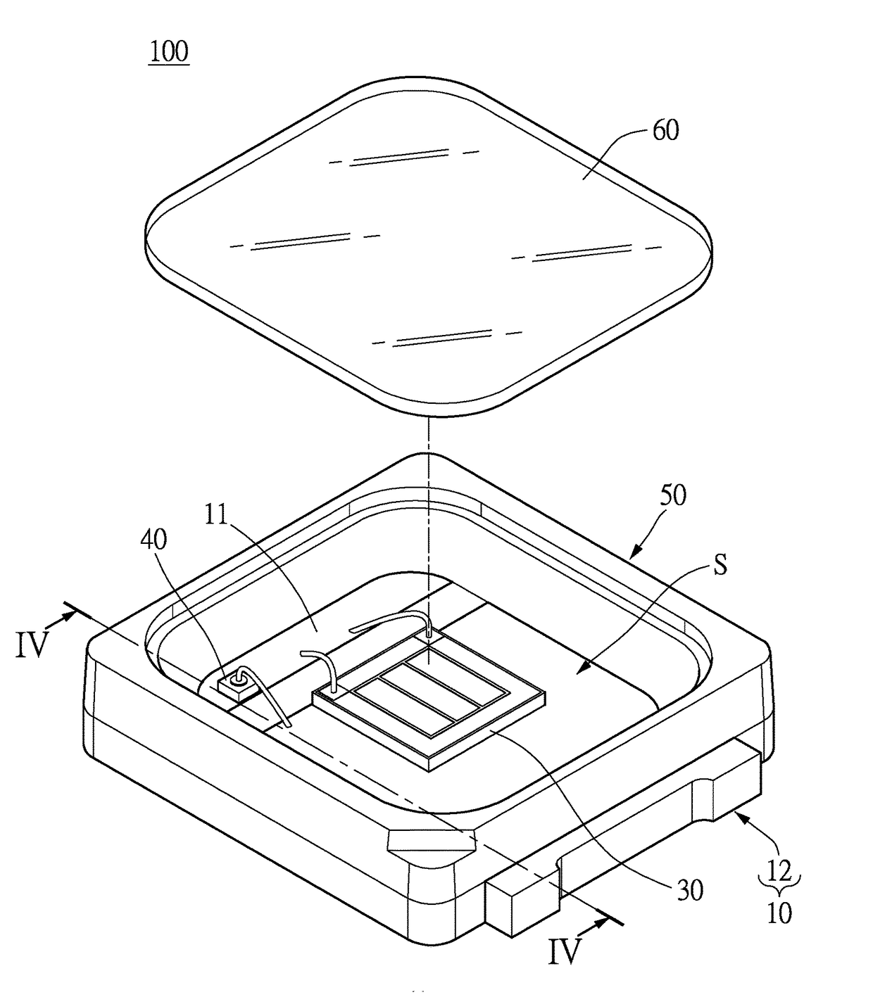
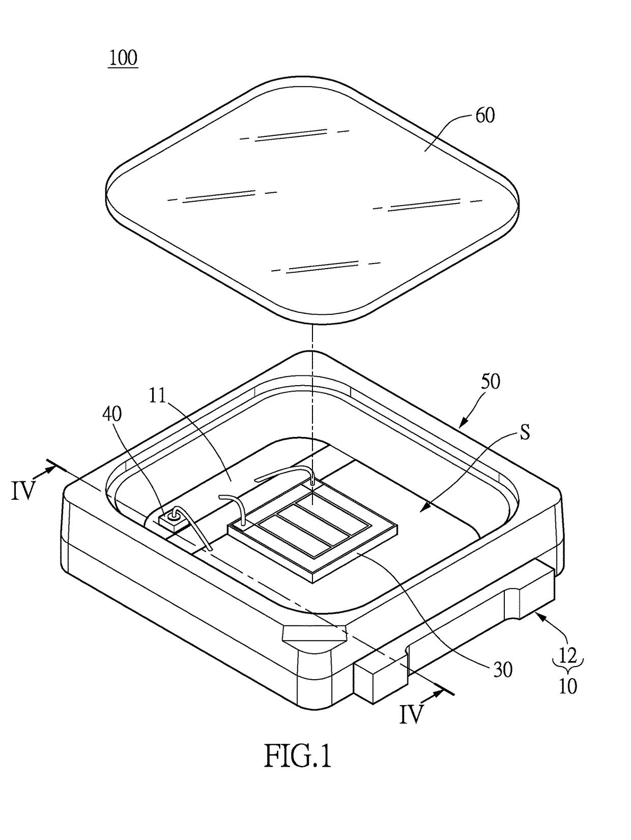
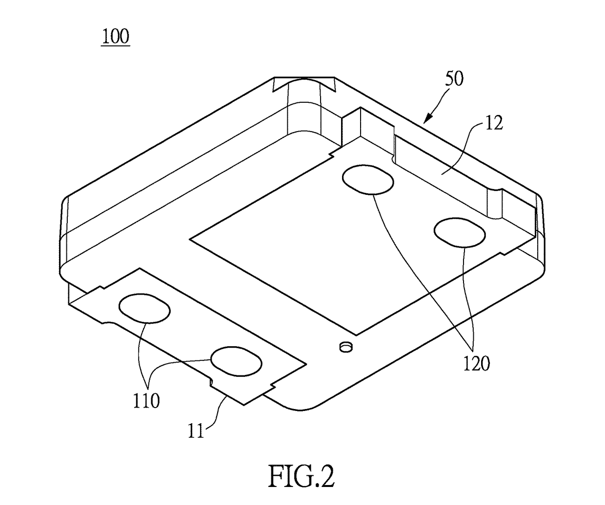
[0018]Please refer to FIGS. 1 to 2, which show the perspective views of an LED package structure of the present disclosure, and FIG. 3, which shows an exploded view of the LED package structure of the present disclosure, an LED package structure 100 of the present disclosure includes a conductive frame assembly 10, a UV LED chip 30, and a reflective housing 50. The reflective housing 50 is combined with the conductive frame assembly 10, and part of the reflective housing 50 protrudes from a top surface of the conductive frame assembly 10 and incorporates with the conductive frame assembly 10 to form an accommodating space S. The UV LED chip 30 emitting the UV light is disposed on the conductive frame assembly 10 and located within the accommodating space S. As shown in FIG. 1 and FIG. 4, a cover 60 may be disposed at a top surface of the reflective housing 50. In other embodiments, as shown in FIG. 4A, an encapsulant 70 may be disposed within the accommodating space S of the reflect...


PUM


Abstract

An LED package structure includes a conductive frame assembly, a reflective housing, an UV LED chip disposed on the conductive frame assembly, and a die-attach adhesive for bonding the UV LED chip to the conductive frame assembly. The reflective housing includes Silicone Molding Compound (SMC) and filler mixed in the SMC. The energy gap of the filler is greater than or equal to 4 eV. The energy gap of the filler thereof can be chosen by the following formulas. When the refractive index difference between the filler and the SMC is less than or equal to 0.2, the energy gap of the filler is satisfied the following formula. E≧1240 (nm·eV) / (λ−150(nm)). When the refractive index difference between the filler and the SMC is greater than 0.2, the energy gap of the filler is satisfied the following formula. E≧1240(nm·eV) / (λ−50(nm)).

Description

TECHNICAL FIELD[0001]The present disclosure relates to an LED package structure, and more particularly to an LED package structure having a conductive frame assembly in combination with a reflective housing using the silicone molding compound.BACKGROUND ART[0002]LED (Light Emitting Diode) has been gradually used as a light source for various purposes. For example, LED emitting visible light is used for general illumination. LED emitting invisible light is used for special illumination, such as UV light is used for curing, sterilization, security identification, and the like.[0003]UV Light emitted from UV LEDs is short-waveband with strong energy, and thus the material requirements of a conductive frame assembly and a reflective housing for a UV LED package structure are more strict, affecting not only the package's lifetime but also its overall light reflectivity.[0004]In order to avoid materials of UV LED package from being degraded due to a long-time UV irradiation, a ceramic subs...

Claims


Application Information

Patent Timeline
Patent Type & Authority Applications(United States)
IPC IPC(8): H01L33/48H01L33/54H01L33/62H01L33/60
CPCH01L33/486H01L33/62H01L33/54H01L33/60H01L2224/48247H01L2933/0033H01L2933/0058
Inventor CHIEN, I-CHENHSU, SHIH-CHANG
Owner LITE ON OPTO TECH (CHANGZHOU) CO LTD
Why Eureka
Try Eureka