

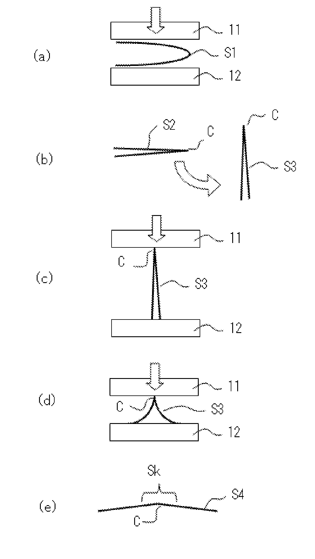
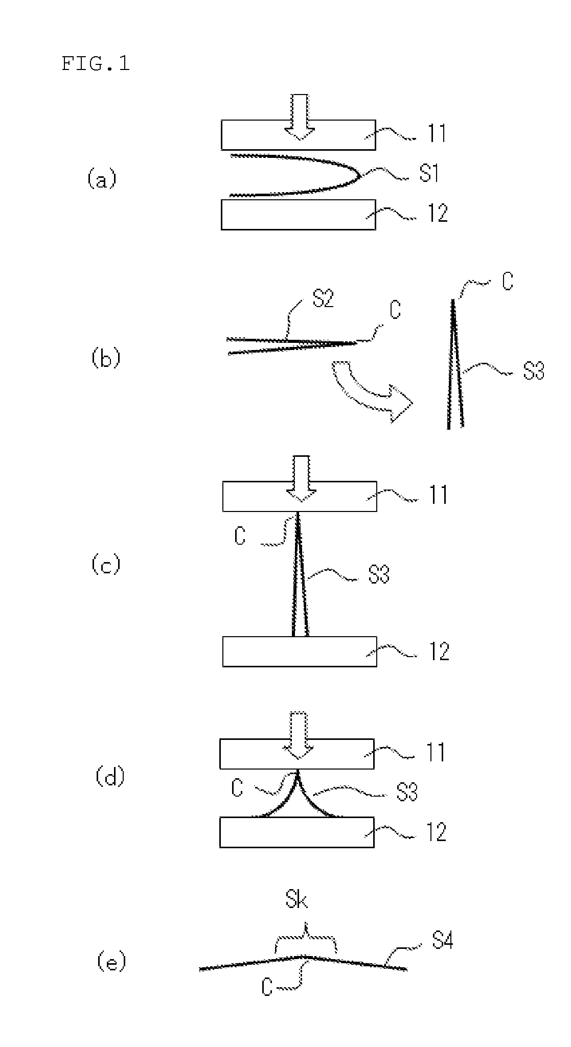
Laminate For Printed Wiring Board, Method Of Manufacturing Printed Wiring Board, And Method Of Manufacturing Electronic Device
a technology of printed wiring and laminate, which is applied in the direction of flexible printed circuits, other domestic objects, chemistry apparatuses and processes, etc., can solve the problems of fine-pitch wiring patterns and limit the application of laminates, and achieve the effect of favorable bending endurance and circuit formability
- Summary
- Abstract
- Description
- Claims
- Application Information
AI Technical Summary
Benefits of technology
Problems solved by technology
Method used
Image

Examples
examples
[0116]In the following descriptions, experimental examples are provided as Examples of the present invention and Comparative Examples. These Examples are provided to give a better understanding of the present invention and its advantages, and therefore these Examples should not be construed as limiting the present invention.
(Production of Laminate for Printed Wiring Board)
[0117]In Examples 1-9 and Comparative Examples 1-4, a polyimide resin (a Upilex 25VT, BPDA (biphenyl-tetracarboxylic acid dianhydride) base (specifically, BPDA-PDA (para-phenylenediamine) base) polyimide resin substrate that is a product of Ube Industries, Ltd.) with a 25-μm-thick adhesion layer (thermal adhesion layer) was used as the insulating resin substrate, and a tough pitch copper (TPC) or an oxygen-free copper (OFC) to which elements of composition provided in Table 1, or a rolled copper foil of a tough pitch copper or an oxygen-free copper (the thickness of the copper foil is provide in Table 1) was used a...
PUM
| Property | Measurement | Unit |
|---|---|---|
| twin particle diameter | aaaaa | aaaaa |
| thickness | aaaaa | aaaaa |
| thickness | aaaaa | aaaaa |
Abstract
Description
Claims
Application Information