
Display device

a technology of display device and display screen, which is applied in the direction of semiconductor devices, basic electric elements, electrical apparatus, etc., can solve the problems of increasing the cost of the patterning process in the manufacturing of the device, and achieve the effect of avoiding the increase of the cost of manufacturing

Active Publication Date: 2017-08-31
JAPAN DISPLAY INC
View PDF8 Cites 17 Cited by
  • Summary
  • Abstract
  • Description
  • Claims
  • Application Information

AI Technical Summary

Benefits of technology

This patent describes a display device that combines the advantages of a white pixel and a micro-cavity structure without adding manufacturing costs. The device includes a light scattering structure in the white pixel to reduce optical interference and make the light emitted from the white pixel pure. Additionally, the device includes different chromatic color pixels with a micro-cavity structure, providing an advantage from this structure as well. The second reflecting layer is formed on both the white and chromatic color pixels, which avoids the need to pattern the semitransparent reflecting layer based on the positions of the white and chromatic color pixels. Overall, this patent provides a display device that offers the benefits of a white pixel and a micro-cavity structure without increasing manufacturing costs.

Problems solved by technology

The patterning process increases cost in manufacturing the device.

Method used


Image

  • Display device
  • Display device
  • Display device

Examples


Embodiment Construction

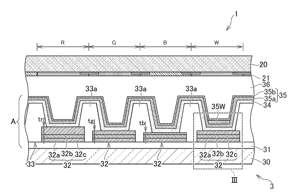
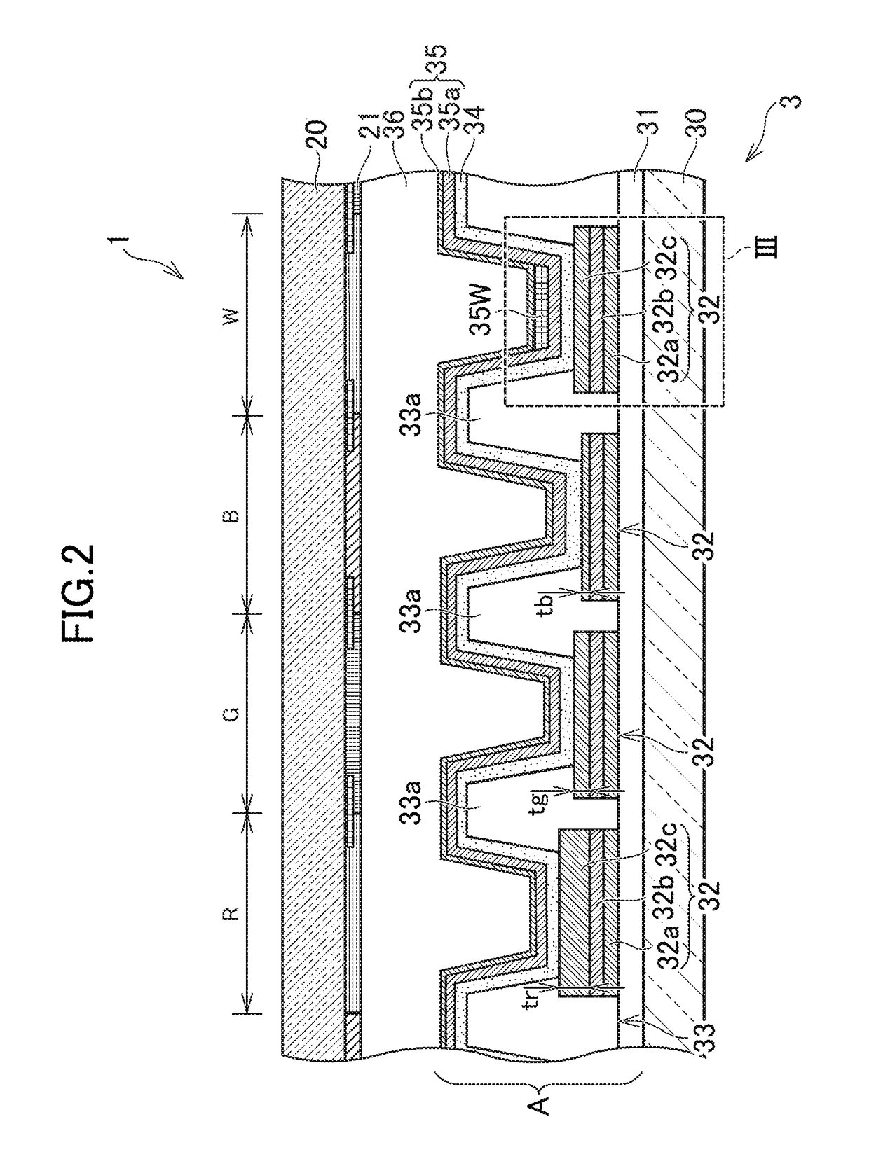
[0017]Hereinafter, embodiments according to the present invention will be described. In the present specification, an organic EL display device including an organic LED (Light Emitting Diode) as a light emitting element will be described as an example of the embodiments. The present invention may be applied to a display device including a quantum dot LED as the light emitting element.

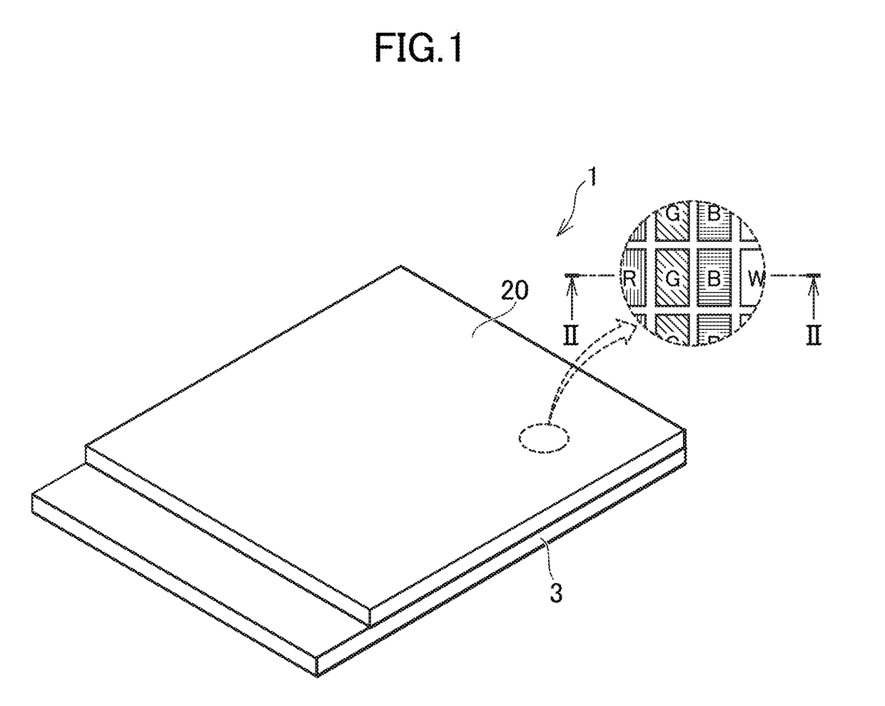
[0018]FIG. 1 illustrates an exemplary organic EL display device of embodiments according to the present invention. FIG. 2 is a cross section taken along line II-II in FIG. 1. In the following description, an “upward direction” means a direction from a display panel 3 to an opposite substrate 20. On the contrary, a “downward direction” means a direction from the opposite substrate 20 to the display panel 3.

[0019]The present specification discloses examples of various embodiments according to the present invention. Embodiments which maintain the spirit of the present invention and are easily modified by t...


PUM


Abstract

The reflecting layer is formed on a white pixel PW and chromatic color pixels PR, PG, and PB. The semitransparent reflecting layer is formed on the white pixel PW and the chromatic color pixels PR, PG, and PB. The semitransparent reflecting layer and the intermediate layer in the white pixel PW constitute the light scattering structure. According to this display device, it is possible to obtain an advantage of a micro-cavity structure and an advantage of the white pixel while suppressing an increase in manufacturing cost.

Description

CROSS-REFERENCE TO RELATED APPLICATION[0001]The present application claims priority from Japanese application JP2016-036009 filed on Feb. 26, 2016, the content of which is hereby incorporated by reference into this application.BACKGROUND OF THE INVENTION[0002]1. Field of the Invention[0003]The present patent specification relates to a display device and more particularly to a display device including pixels that employs light-emitting elements such as organic electroluminescent (EL) elements.[0004]2. Description of the Related Art[0005]Some organic EL display devices have an optical micro-cavity structure where a distance between a reflecting layer and a semitransparent reflecting layer in pixels is regulated according to wavelength of light emitted from a light emitting layer. In most of the devices, the reflecting layer and the semitransparent reflecting layer are employed as electrodes, and the light emitting layer is formed between the reflecting layer and the semitransparent re...

Claims


Application Information

Patent Timeline
Patent Type & Authority Applications(United States)
IPC IPC(8): H01L27/32H01L51/52
CPCH01L27/3213H01L51/5268H01L51/5271H10K59/351H10K59/878H10K59/877H10K59/876H10K50/11H10K50/852H10K50/854H10K50/856H10K59/35H10K59/122H10K59/131H10K2101/10
Inventor USHIKUBO, TAKAHIRO
Owner JAPAN DISPLAY INC
Features
  • Generate Ideas
  • Intellectual Property
  • Life Sciences
  • Materials
  • Tech Scout
  • Unparalleled Data Quality
  • Higher Quality Content
  • 60% Fewer Hallucinations
Learn More