Optical communication system and optical transmitter

a communication system and optical transmitter technology, applied in the field of optical communication technology, can solve the problems of limited transmission capacity and difficult density wavelength division multiplexing, and achieve the effect of suppressing the deterioration of intensity waveform, improving bit error ratio and receiver sensitivity

Active Publication Date: 2017-08-31
LUMENTUM JAPAN INC
View PDF10 Cites 25 Cited by
  • Summary
  • Abstract
  • Description
  • Claims
  • Application Information

AI Technical Summary

Benefits of technology

[0016]The optical receiver section 103 includes a local-oscillator laser source 182, a polarization demultiplexing 90° optical hybrid 183, four balanced PD modules 184, four AD converters 185, a polarization demultiplexing butterfly filter 186, a frequency / phase estimation circuit 187, and a binary decision circuit 188. The received light (SSB modulated optical signal) received from the optical transmission section 104 by the optical receiver section 103 is multiplexed with local oscillation light emitted from the local-oscillator laser source 182 by the polarization demultiplexing 90° optical hybrid 183. Then, the multiplexed light is demultiplexed into four signals, which are respectively input to the four balanced PD modules 184 to be converted into electronic signals. A real-part component (XI) and an imaginary-part component (XQ) of an X-polarized component of the received light and a real-part component (YI) and an imaginary-part component (YQ) of a Y-polarized component of the received light are respectively converted into the electronic signals, output from the four balanced PD modules 184, and input to the four AD converters 185. Those electronic signals are converted into digital signals by the four AD converters 185, and input to the polarization demultiplexing butterfly filter 186. The polarization demultiplexing butterfly filter 186 adaptively subjects the input signals to polarization separation and equalization. An output signal from the polarization demultiplexing butterfly filter 186 is input to the frequency / phase estimation circuit 187. An output signal from the frequency / phase estimation circuit 187 is input to the binary decision circuit 188 to be decoded. The output signal (transmission light electric field) from the frequency / phase estimation circuit 187 exhibits a wide spread along the imaginary axis (Q axis) direction as shown in FIG. 18B(b), but the binary decision circuit 188 conducts binary decision from a real-axis (I-axis) component of the output signal, and therefore can restore its original information signal.
[0017]However, the optical communication system according to the related art illustrated in FIG. 15 is complicated in the modulation and demodulation of a signal, in particular, complicated in the configuration of the optical receiver section 103, and thus leads to increases in the cost, the size, and the power consumption of the optical communication system.
[0019]As described above, when the Hilbert transformation is approximated by a low-order filter, the deterioration in receiver sensitivity can be suppressed to a certain extent, but it is difficult to increase the side-band suppression ratio. Meanwhile, when a high-order filter is used to improve approximation accuracy of the Hilbert transformation, the side-band suppression ratio can be improved, but the intensity of an imaginary-part component given by the Hilbert transformation can no longer be ignored, which causes a large waveform distortion.
[0021]The present invention has been made in view of the above-mentioned problems, and has an object to provide an optical communication system capable of suppressing the deterioration of an intensity waveform of an optical intensity modulated signal subjected to transformation using SSB modulation and improving a bit error ratio and a receiver sensitivity of the optical intensity modulated signal, and an optical transmitter used for the optical communication system.
[0032]According to the present invention, there are provided the optical communication system capable of suppressing the deterioration of the intensity waveform of the optical intensity modulated signal subjected to the transformation using SSB modulation and improving the bit error ratio and the receiver sensitivity of the optical intensity modulated signal, and the optical transmitter used for the optical communication system.

Problems solved by technology

Therefore, there is a problem in that dense wavelength division multiplexing is difficult due to low frequency utilization efficiency, which imposes a limitation on transmission capacity.

Method used


Image

  • Optical communication system and optical transmitter
  • Optical communication system and optical transmitter
  • Optical communication system and optical transmitter

Examples


first embodiment

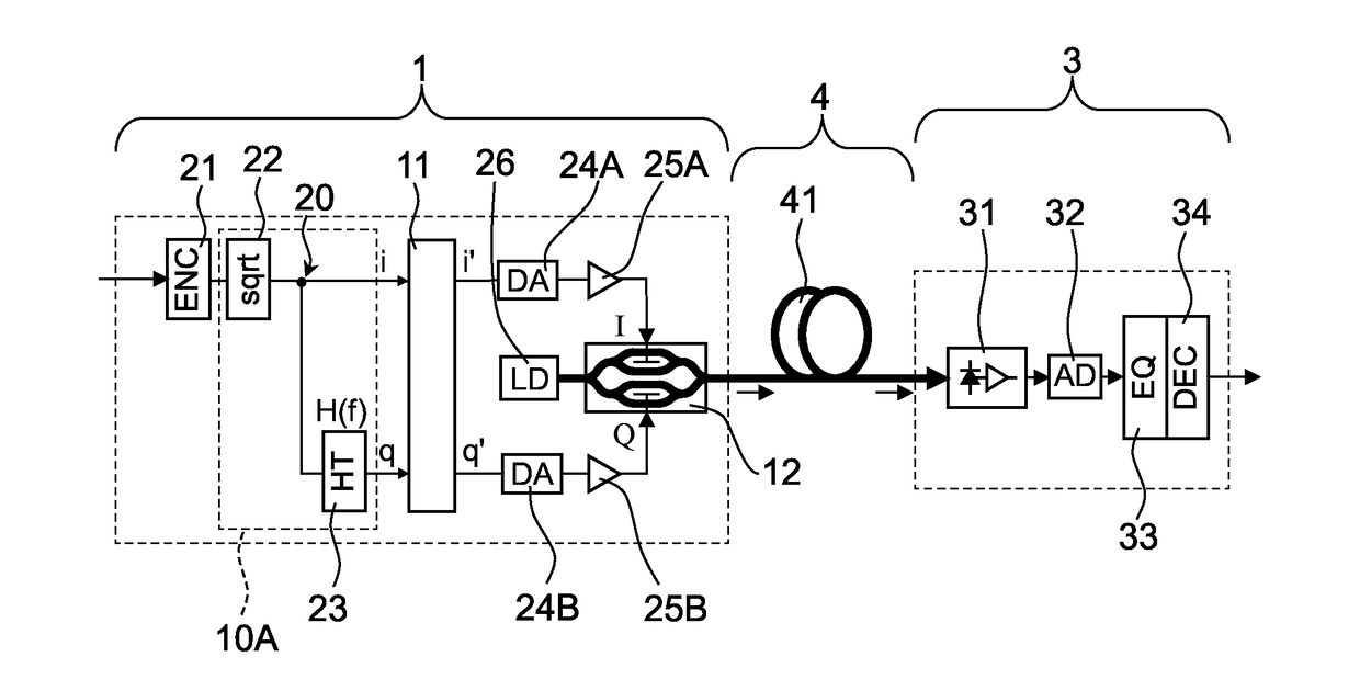
[0058]FIG. 1 is a schematic diagram for illustrating a configuration of an optical communication system according to a first embodiment of the present invention. The optical communication system according to this embodiment is configured to transmit an optical signal subjected to optical multi-level baseband intensity modulation through an optical fiber transmission line having a relatively short transmission distance of from several hundred meters to several tens of kilometers. The optical communication system according to this embodiment includes an optical transmitter section 1, an optical receiver section 3, and an optical transmission section 4.

[0059]The optical transmitter section 1 is an SSB optical pulse amplitude modulation transmitter, and includes a waveform distortion correction circuit 11, an optical IQ modulator 12, a branch point 20, a multi-level coding circuit 21, a square rooting circuit 22, a Hilbert transformer 23, two DA converters 24A and 24B, two driver amplif...

second embodiment

[0075]FIG. 3 is a schematic diagram for illustrating a configuration of the optical transmitter section 1 according to a second embodiment of the present invention. The optical communication system according to this embodiment is the same as the optical communication system according to the first embodiment except that the optical transmitter section 1 has a different configuration. Specifically, the square rooting circuit 22 is arranged in a different position, and in accordance with the difference, configurations of a waveform distortion correction circuit 13 and an optical IQ modulator 14 are different. An SSB modulation transformation circuit 10B according to this embodiment includes the branch point 20, the square rooting circuit 22, and the Hilbert transformer 23.

[0076]As illustrated in FIG. 3, in the optical transmitter section 1, the multi-level coding circuit 21 outputs a quaternary code. The quaternary code is divided into two signals at the branch point 20, and one signal...

third embodiment

[0080]FIG. 5 is a schematic diagram for illustrating a configuration of the optical transmitter section 1 according to a third embodiment of the present invention. The optical communication system according to this embodiment is the same as the optical communication system according to the second embodiment except that the optical transmitter section 1 further includes a Nyquist filter 51 having a Nyquist filter transmission characteristic. In the optical transmitter section 1, the Nyquist filter 51 is arranged in the subsequent stage of the multi-level coding circuit 21. An SSB modulation transformation circuit 10C according to this embodiment includes the branch point 20, the square rooting circuit 22, the Hilbert transformer 23, and the Nyquist filter 51. With this configuration, optical Nyquist modulation that further constricts the band of the optical signal is achieved. The Nyquist modulation is a technology for reducing the signal frequency band by about ½ by forming an elect...


PUM


Abstract

Provided is an optical communication system capable of suppressing the deterioration of an intensity waveform of an optical intensity modulated signal subjected to transformation using SSB modulation and improving a bit error ratio and a receiver sensitivity of the optical intensity modulated signal. The optical communication system includes: an optical transmitter section including: a single-side band modulation circuit configured to subject a double-side band modulated signal to generate a single-side band modulated signal; a correction circuit configured to correct an intensity of the single-side band modulated signal so that the intensity of the single-side band modulated signal becomes closer to an intensity of the double-side band modulated signal; and an optical IQ modulator configured to output an optical modulated signal; and an optical receiver section configured to receive the optical modulated signal to directly detect an intensity component of the optical modulated signal.

Description

CROSS-REFERENCE TO RELATED APPLICATION[0001]The present application claims priority from Japanese application JP 2016-038256, filed on Feb. 29, 2016, the content of which is hereby incorporated by reference into this application.BACKGROUND OF THE INVENTION[0002]1. Field of the Invention[0003]The present invention relates to an optical communication technology, and more particularly, to an optical communication system suitable for transmission of an optical signal and an optical transmitter used for the optical communication system.[0004]2. Description of the Related Art[0005]In an optical communication technology, there are increasing demands for further cost reduction, simplification, downsizing, and lower power consumption of an optical transmitter and an optical receiver in addition to a speedup of optical communications. In order to meet such demands, an optical communication system using intensity modulation / direct detection (IM / DD) with a simplified configuration is suitable. ...

Claims


Application Information

Patent Timeline
Patent Type & Authority Applications(United States)
IPC IPC(8): H04B10/54H04J14/02H04B10/2513
CPCH04B10/54H04J14/02H04B10/2513H04B10/2507H04B10/5165H04B10/61
Inventor KIKUCHI, NOBUHIKO
Owner LUMENTUM JAPAN INC
Why Eureka
Try Eureka