Developing device

Active Publication Date: 2017-09-07
CANON KK
View PDF3 Cites 5 Cited by
  • Summary
  • Abstract
  • Description
  • Claims
  • Application Information

AI Technical Summary

Benefits of technology

The present invention aims to provide a developing device that can accurately detect the amount of toner in a developer using an inductance sensor with a planar coil. The main goal is to improve the detection sensitivity and accuracy of the sensor.

Problems solved by technology

The toner contained in the developer is consumed by being subjected to development, and therefore a toner content of the developer in a developing container lowers with use for a long time.
However, when the toner content of the developer is not maintained within a roller range, image defect can generate during image formation.
However, in this case, although the magnetic field penetrating through the substrate is generated by the coil depending on the energization, i.e., the magnetic field generates on both surfaces (both sides) of the detecting member, the change in magnetic field is detected only at one surface of the detecting member, and therefore the detection sensitivity of the sensor is liable to lower.
Further, an amount of the developer to be detected is small by the detection at one surface, and therefore detection accuracy of the sensor is liable to lower.
However, in a conventional developing device disclosed in JP-A 2012-14034, one surface of the detecting member contacts the developer in the developing chamber and the other surface of the detecting member contacts the developer in the stirring chamber thereby to detect the change in magnetic field, and therefore a detection result is liable to change by the influence of toner content (density) non-uniformity which can vary depending on each of the chambers.
Therefore, in the conventional developing devices, the toner content of the developer was not able to be property detected, with the result that it was difficult to maintain the toner content within the predetermined range.

Method used


Image

  • Developing device
  • Developing device
  • Developing device

Examples


example 1

Conventional Example 1

[0056]In the case of Conventional Example 1 shown in FIG. 12, the inductance sensor 90 is provided along an inner wall surface of the developing container 40 in the stirring chamber 40b so as to oppose the stirring screw 45 in a downstream side with respect to a developer feeding direction of the stirring screw 45. Further, the inductance sensor 90 is provided so that one surface of the detecting portion 90a where the planar coil 92 is formed faces an inside (the stirring screw 45 side) of the developing container 40 so that the planar coil 92 contacts the developer in the developing container 40. In this case, the developer is liable to stagnate between the planar coil 92 of the inductance sensor 90 and the stirring screw 45, so that an immovable layer of the developer is liable to be formed. For that reason, in the case of Conventional Example 1, only at a position where replacement of the developer does not readily generate, i.e., at a position where flowabi...

example 2

Conventional Example 2

[0057]In the case of Conventional Example 2 shown in FIG. 13, the inductance sensor 90 is provided on an outer wall surface of the stirring chamber 40b of the developing container 40 so that the planar coil 92 does not contact the developer in the developing container 40. Further, the inductance sensor 90 is provided so that one surface of the detecting portion 90a where the planar coil 92 is formed faces the developing container 40. This is because it is difficult to detect the change in magnetic field due to permeability of the developer when the magnetic field generated by the planar coil 92 does not have the influence on the developer in the stirring chamber 40b. Therefore, in the case of Conventional Example 2, it is preferable that a current larger than the current in Conventional Example 1 is caused to flow through the planar coil 92 so that the magnetic field generated by the planar coil 92 has the influence on the developer in the stirring chamber 40b ...

first embodiment

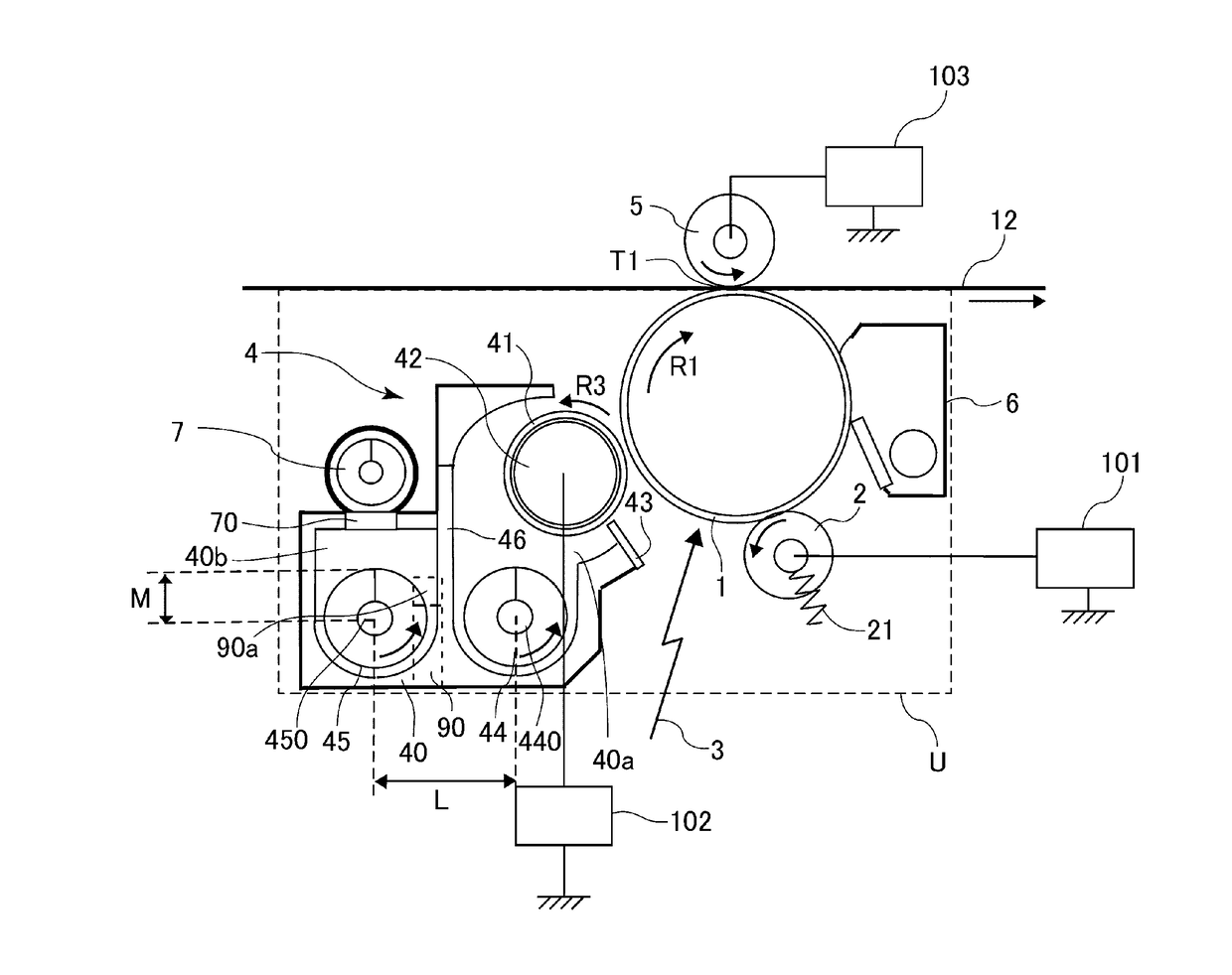
[0059]On the other hand, in the developing device 4 in this embodiment, the inductance sensor 90 is provided so that the change in magnetic field can be detected at both surfaces (both sides) of the detecting portion 90a, i.e., the planar coil 92. In this embodiment, as regards the inductance sensor 90, the detecting portion 90a where the planar coil 92 is formed is disposed in the developing container 40, while a circuit portion 90b electrically connected with the planar coil 92 is disposed outside the developing container 40. In the following, an arrangement of the inductance sensor 90 in the developing device 4 in this embodiment, particularly an arrangement of the detecting portion 90a will be described using FIGS. 3 and 9.

[0060]As shown in FIG. 9, the developing screw 44 is provided with a first helical blade 441, formed around a rotation shaft 440, for feeding the developer in an arrow A direction in the figure. On the other hand, the stirring screw 45 is provided with a secon...


PUM


Abstract

A developing device includes a rotatable developer carrying member, first and second chambers, a first rotatable feeding member, a second rotatable feeding member, a first communication port, a second communication port, and a toner content detecting portion including a planar detecting surface including at least a planar coil. The detecting surface is provided in a region of the first communication port sandwiched between rotational axes of the first and second rotatable feeding members and is disposed at a position such that the developer is fed toward both sides of the toner content detecting portion in a direction in which the detecting surface crosses the first direction.

Description

FIELD OF THE INVENTION AND RELATED ART[0001]The present invention relates to a developing device suitable for an image forming apparatus, using electrophotography, such as a copying machine, a printer, a facsimile machine or a multi-function machine.[0002]In the developing device used in the image forming apparatus such as the copying machine, the printer, the facsimile machine or the multi-function machine, a two-component developer consisting of non-magnetic toner and a magnetic carrier (hereinafter, the developer is simply referred to as a developer). The toner contained in the developer is consumed by being subjected to development, and therefore a toner content of the developer in a developing container lowers with use for a long time. However, when the toner content of the developer is not maintained within a roller range, image defect can generate during image formation. Therefore, a developing device capable of maintaining the toner content of the developer subjected to deve...

Claims


Application Information

Patent Timeline
IPC IPC(8): G03G15/08
CPCG03G15/0891G03G15/0853G03G15/09G03G15/0893G03G2215/0838
Inventor SUZUKI, SHINYA
Owner CANON KK
Why Eureka
Try Eureka