
Output circuit

a technology of output circuit and output circuit, which is applied in the field of output circuit, can solve the problems of high speed and difficulty in switching operation of pmos transistor b>612/b>, and achieve the effect of stable and high-speed switching operation

Active Publication Date: 2017-09-07
ABLIC INC
View PDF7 Cites 0 Cited by
  • Summary
  • Abstract
  • Description
  • Claims
  • Application Information

AI Technical Summary

Benefits of technology

The present invention provides an output circuit that includes a control voltage generating circuit and four MOS transistors. The control voltage generating circuit generates a control voltage, which is stable and maintained at a predetermined voltage level. The four MOS transistors work together to absorb fluctuations in control voltage and maintain a stable voltage level. This results in high-speed switching operation. Therefore, the technical effect of the invention is to provide a stable and high-speed output circuit for efficient and reliable electronic devices.

Problems solved by technology

However, the related-art output circuit 600 as described above has a problem in that it is difficult to perform switching operation of the PMOS transistor 612 at high speed.

Method used


Image

  • Output circuit
  • Output circuit
  • Output circuit

Examples


Embodiment Construction

[0029]Now, an embodiment of the present invention is described with reference to the drawings.

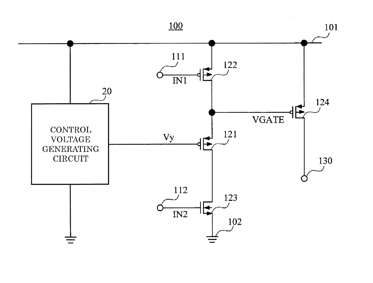
[0030]FIG. 1 is a circuit diagram of an output circuit 100 according to the embodiment of the present invention.

[0031]The output circuit 100 of this embodiment includes a power supply terminal (also referred to as “first power supply terminal”) 101, a ground terminal 102 (also referred to as “second power supply terminal”), a first input terminal 111, a second input terminal 112, PMOS transistors 121, 122, and 124, an NMOS transistor 123, an output terminal 130, and a control voltage generating circuit 20.

[0032]The PMOS transistor 124 has a source connected to the power supply terminal 101, and a drain connected to the output terminal 130. The PMOS transistor 122 has a source connected to the power supply terminal 101, and a gate connected to the first input terminal 111. The PMOS transistor 121 has a source connected to a drain of the PMOS transistor 122 and a gate of the PMOS transistor 1...


PUM


Abstract

The output circuit includes: a control voltage generating circuit configured to generate a control voltage; a first MOS transistor having a gate for receiving the control voltage; a second MOS transistor having a gate to which a first input signal is input; a third MOS transistor having a gate to which a second input signal is input; and a fourth MOS transistor which has a gate connected to a source of the first MOS transistor, and a drain connected to an output terminal, and is configured to be driven with the first input signal and the second input signal to output an output signal to the output terminal. The control voltage generating circuit is configured to absorb fluctuations in control voltage, which are caused due to changes in first input signal and second input signal, to thereby maintain the control voltage at a predetermined voltage.

Description

RELATED APPLICATIONS[0001]This application claims priority under 35 U.S.C. §119 to Japanese Patent Application No. 2016-043655 filed on Mar. 7, 2016, the entire content of which is hereby incorporated by reference.BACKGROUND OF THE INVENTION[0002]1. Field of the Invention[0003]The present invention relates to an output circuit, and more particularly, to an output circuit configured to perform control of turning on / off a MOS transistor connected to high voltage using a low voltage signal, to thereby generate an output signal.[0004]2. Description of the Related Art[0005]Output circuits that generate an output signal for driving a load operating under a high voltage of several tens of volts are, for example, configured to turn on / off a MOS transistor connected to high voltage using a low voltage signal, to thereby obtain an output signal at high voltage from the MOS transistor.[0006]As an example of such output circuits, a related-art output circuit 600 is illustrated in a circuit diag...

Claims


Application Information

Patent Timeline
Patent Type & Authority Applications(United States)
IPC IPC(8): G05F3/16H03K17/041
CPCH03K17/04106G05F3/16G05F1/561H03K17/08122H03K17/6872H03K19/0948
Inventor TAKADA, KOSUKE
Owner ABLIC INC
Learn More