

Solid state imaging device including a semiconductor substrate on which a plurality of pixel cells have been formed
a semiconductor substrate and solid-state imaging technology, which is applied in the direction of picture signal generators, television systems, radioation controlled devices, etc., can solve the problems of two pixels, large shading in the output signal, and sensitivity difference between photodiodes, and achieve high-speed effects
- Summary
- Abstract
- Description
- Claims
- Application Information
AI Technical Summary
Benefits of technology
Problems solved by technology
Method used
Image

Examples
embodiment 1
1. Overall Structure
[0042]The following describes the overall structure of a MOS type solid state imaging device 1 according to the present embodiment, with reference to FIG. 4. The MOS type solid state imaging device 1 shown in FIG. 4 is used as an image input device such as a digital still camera or a digital movie camera.
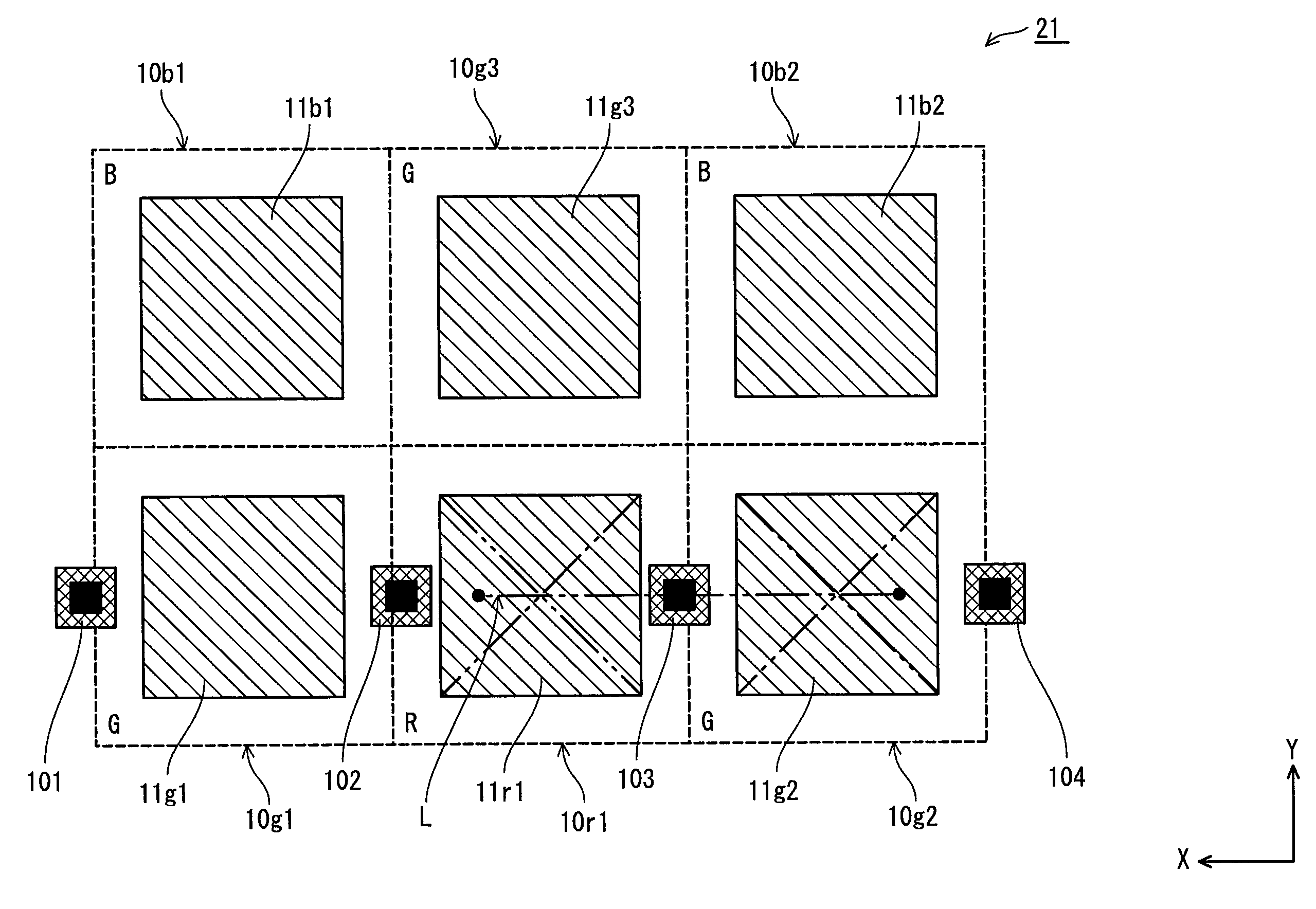
[0043]As shown in FIG. 4, the MOS type solid state imaging device 1 according to embodiment 1 includes a pixel region 21 and a periphery circuit portion. The pixel region 21 is formed from a plurality of pixel cells 10, and the periphery circuit portion has been arranged on the periphery of the pixel region 21 so as to drive the pixel cells 10 in the pixel region 21. The periphery circuit portion includes a vertical scanning circuit 22, a read circuit 23, a horizontal scanning circuit 24 and a load circuit 25.
[0044]The plurality of pixel cells 10, which constitute the pixel region 21, have been arranged two-dimensionally in a semiconductor substrate. Note that, a...
embodiment 2
[0080]The following describes the structure of a MOS type solid state imaging device according to embodiment 2, with reference to FIGS. 11 and 12. Note that each of FIGS. 11 and 12 shows some of pixel cells 40 (40a, 40b, and 40c) in a pixel region 51. The rest of the structure of the MOS type solid state imaging device according to embodiment 2 is basically the same as that of the MOS type solid state imaging device 1 according to embodiment 1 described above.
[0081]As shown in FIG. 11, two photodiodes, namely photodiodes 11 and 41 have been formed in each of the pixel cells 40, in the MOS type solid state imaging device according to embodiment 2. Also, transfer transistors 12 and 42 have been formed with respect to the photodiodes 11 and 41 in each pixel cell 40. The rest of the structure of each pixel cell 40 is the same as that of each pixel cell 10.
[0082]As shown in FIG. 12, when three pixel cells, namely pixel cells 40a, 40b, and 40c are seen by being extracted from the pixel re...
PUM
 Abstract
Description
Claims
Application Information