Quantum dot color film substrate, manufacturing method thereof and LCD apparatus
- Summary
- Abstract
- Description
- Claims
- Application Information
AI Technical Summary
Benefits of technology
Problems solved by technology
Method used
Image
Examples
Embodiment Construction
[0028]To further explain the technical means and effect of the present invention, the following refers to embodiments and drawings for detailed description.
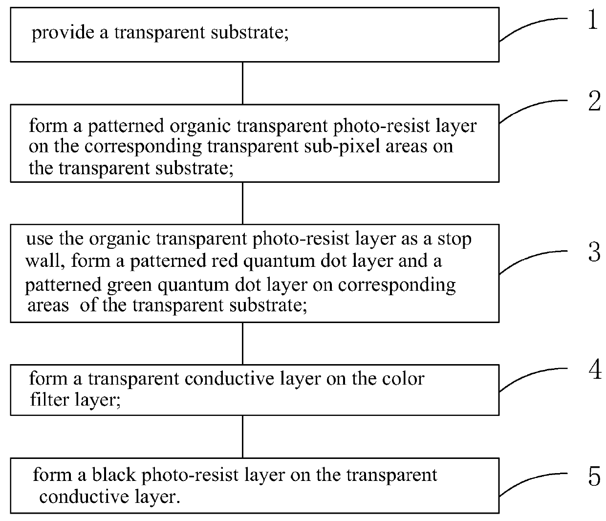
[0029]Refer to FIG. 1. The present invention provides a manufacturing method for quantum dot color film substrate, which comprises:
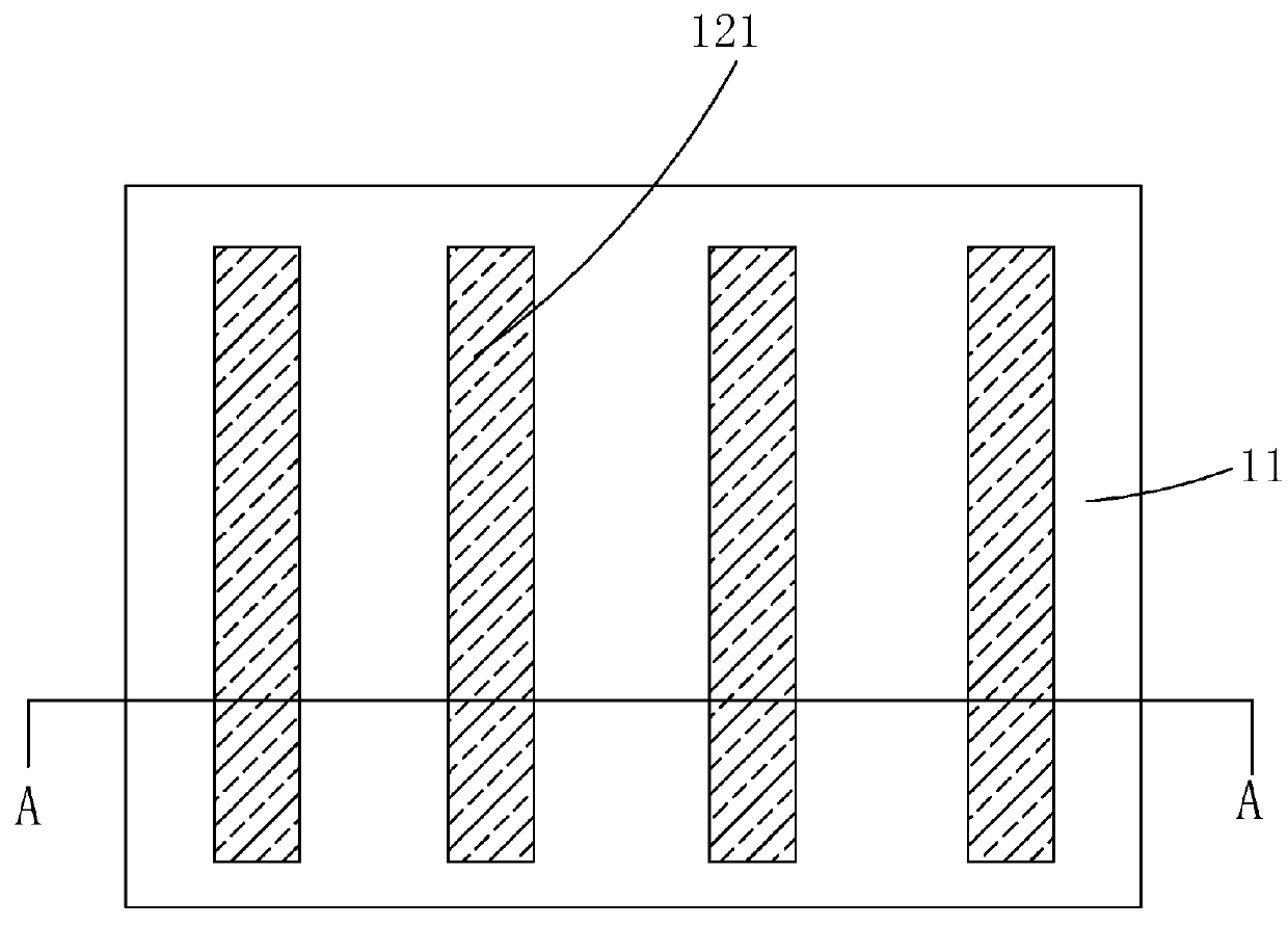
[0030]Step 1: providing a transparent substrate 11.
[0031]Dividing the transparent substrate 11 into a plurality of pixel areas, with each pixel area comprising a red sub-pixel area, a green sub-pixel area, and a transparent sub-pixel area; on the transparent substrate 11, the red sub-pixel area and the green sub-pixel area being separated by the transparent sub-pixel area, with each red sub-pixel area located between two transparent sub-pixel areas, and each green sub-pixel area being located between two transparent sub-pixel areas.
[0032]Specifically, when the quantum dot color film is applied to the display for displaying, the white dot color coordinates are adjusted to within the target range (0.25<...
PUM
| Property | Measurement | Unit |
|---|---|---|
| Thickness | aaaaa | aaaaa |
| Nanoscale particle size | aaaaa | aaaaa |
| Color | aaaaa | aaaaa |
Abstract
Description
Claims
Application Information


