


Quick Research
Generate reliable direction feasibility study reports for your R&D in just a few steps.

Technical Q&A
Discover and master advanced knowledge NOW. Basics, ideas, possibilities, all at once.

Find Solutions
As an expert in R&D theories, this can generate solutions to your technical problems instantly.

Evaluate Feasibility
Analyze your overall solution with one click, know your potential R&D risks in advance.

Monitor Landscape
Get weekly tech updates, stay abreast of the latest tech innovations and key insights.
Semiconductor package with wettable flank
a technology of semiconductor devices and flanks, applied in the direction of semiconductor devices, semiconductor/solid-state device details, electrical apparatus, etc., can solve the problems of further limited space for solder joints, weakened solder joints between the package and the pcb
- Summary
- Abstract
- Description
- Claims
- Application Information
AI Technical Summary
Benefits of technology
Problems solved by technology
Method used
Image

Examples
Embodiment Construction
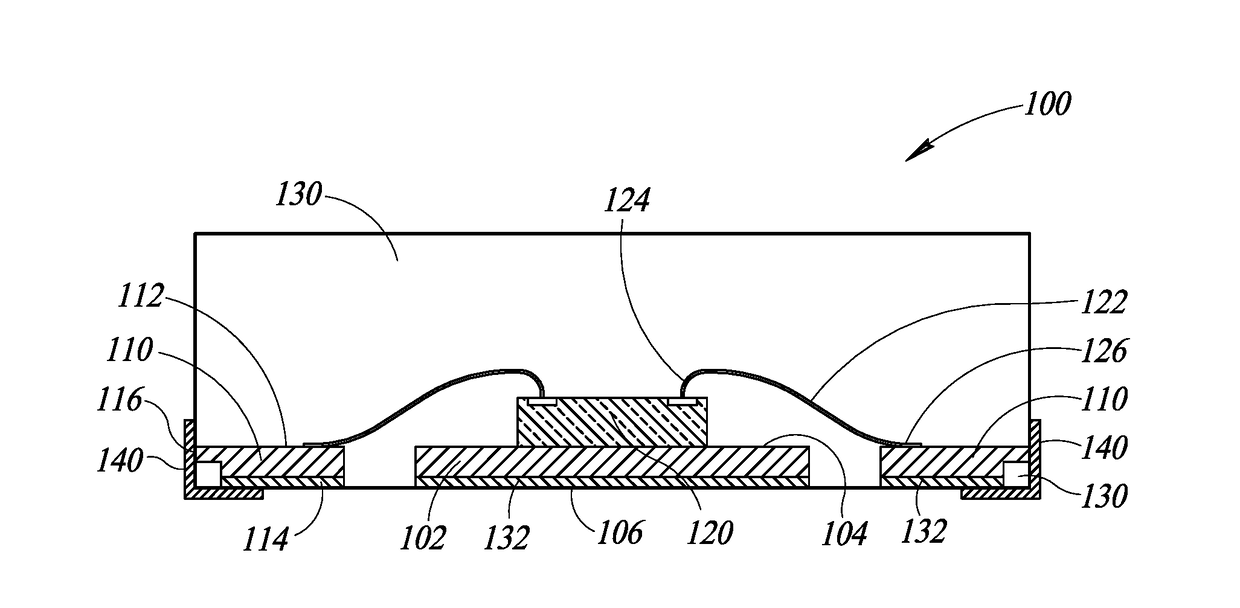
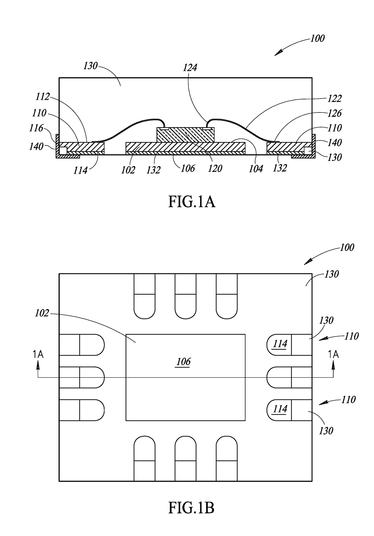
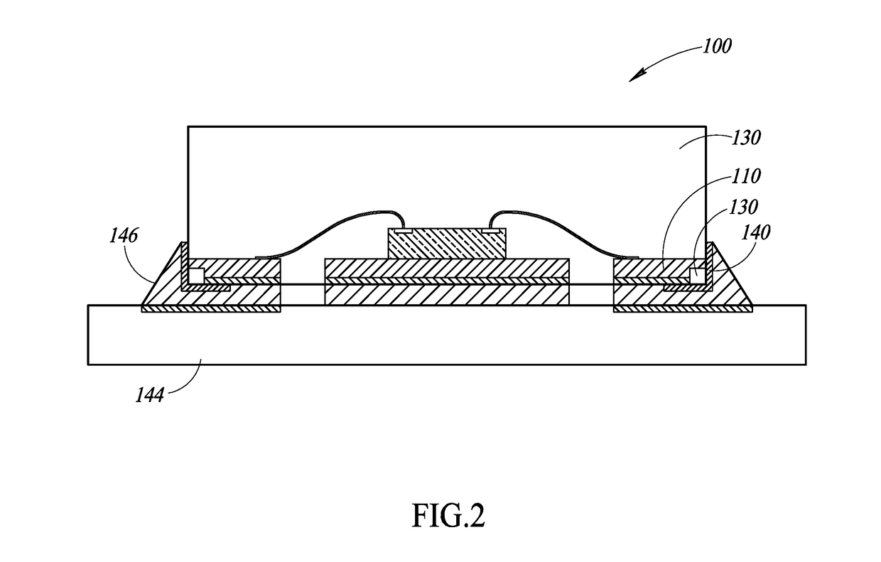
[0010]FIG. 1A shows a cross-sectional view of a QFN leadframe package 100 in accordance with one embodiment of the disclosure. FIG. 1B is a bottom plan view of the package 100. The package 100 includes a die pad 102 having inner and outer surfaces 104, 106. The package 100 further includes a plurality of leads 110, each having inner, bottom, and lateral surfaces 112, 114, 116. The die pad 102 and the leads 110 are formed from a leadframe, which is made of conductive material, typically copper or a copper alloy.
[0011]The leads 110 are located around the die pad 102 and form a recess at the corners of the package 100 where side surfaces of the package 100 meet with a bottom surface of the package 100. Due to the recess, first portions of the leads 110 proximate the lateral surface 116 of the leads 110 have first thicknesses, while second portions of the leads 110 proximate the bottom surface 114 of the leads 110 have second, different thicknesses. The first thicknesses of the first po...
PUM
 Abstract
Description
Claims
Application Information
 - R&D Engineer
- R&D Manager
- IP Professional
- Industry Leading Data Capabilities
- Powerful AI technology
- Patent DNA Extraction
Browse by: Latest US Patents, China's latest patents, Technical Efficacy Thesaurus, Application Domain, Technology Topic, Popular Technical Reports.
© 2024 PatSnap. All rights reserved.Legal|Privacy policy|Modern Slavery Act Transparency Statement|Sitemap|About US| Contact US: help@patsnap.com