Mounting jig for semiconductor device

Active Publication Date: 2017-11-23
FUJI ELECTRIC CO LTD
View PDF0 Cites 1 Cited by
  • Summary
  • Abstract
  • Description
  • Claims
  • Application Information

AI Technical Summary

Benefits of technology

[0012]According to the invention, an insulated circuit board and a plurality of tubular contact elements are positioned by an insulated circuit board positioning jig and a tubular contact element positioning jig, respectively, of a mounting jig, and the tub

Problems solved by technology

Poor positioning accuracy sometimes causes the tubular contact element to be mounted on the insulated circuit board inclined at some angle rather than vertical.
The tubular contact element

Method used


Image

  • Mounting jig for semiconductor device
  • Mounting jig for semiconductor device
  • Mounting jig for semiconductor device

Examples


Example

[0029]An embodiment of each of a manufacturing method of a semiconductor device and a mounting jig according to the invention will be specifically explained with the drawings.

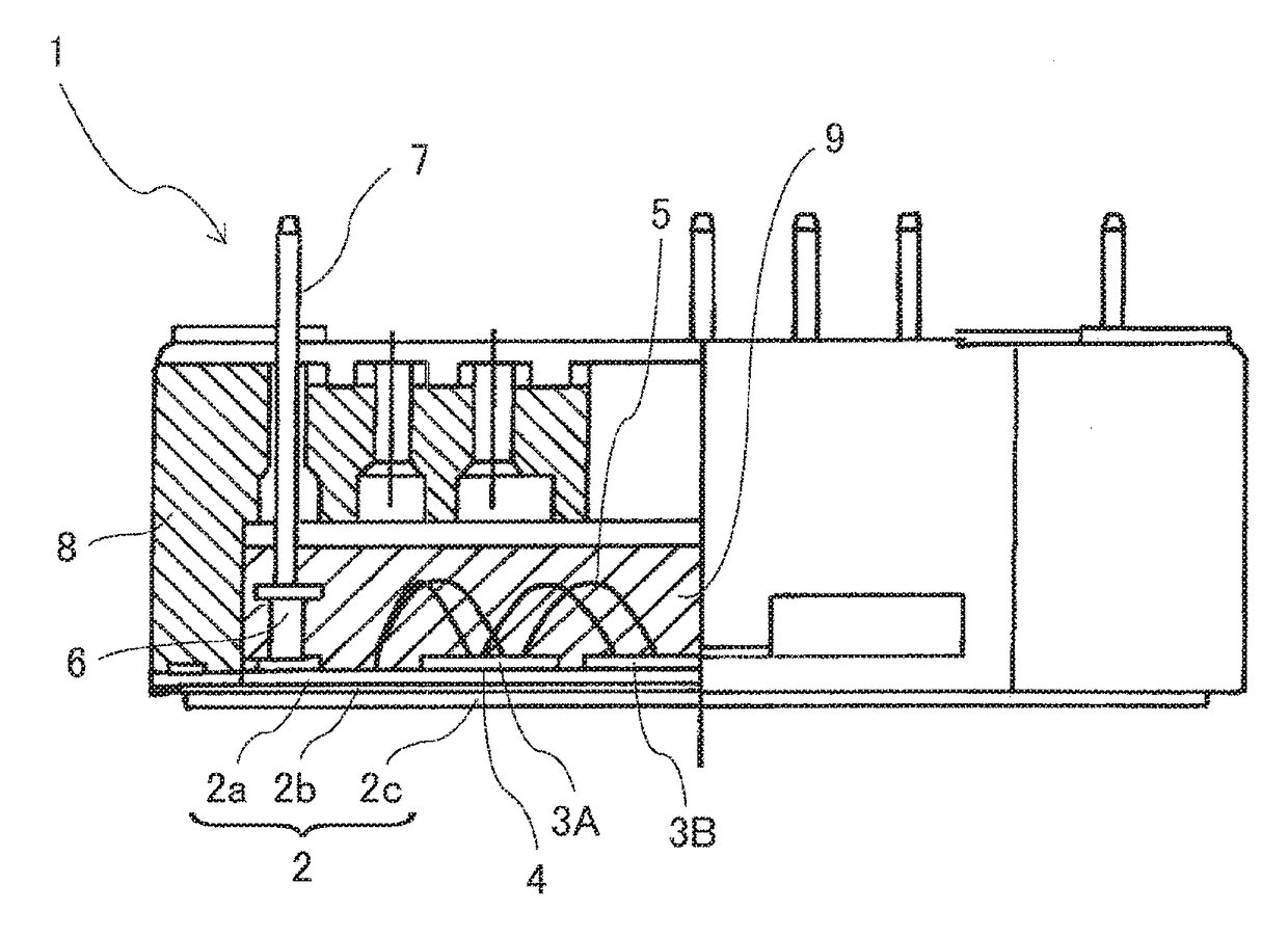
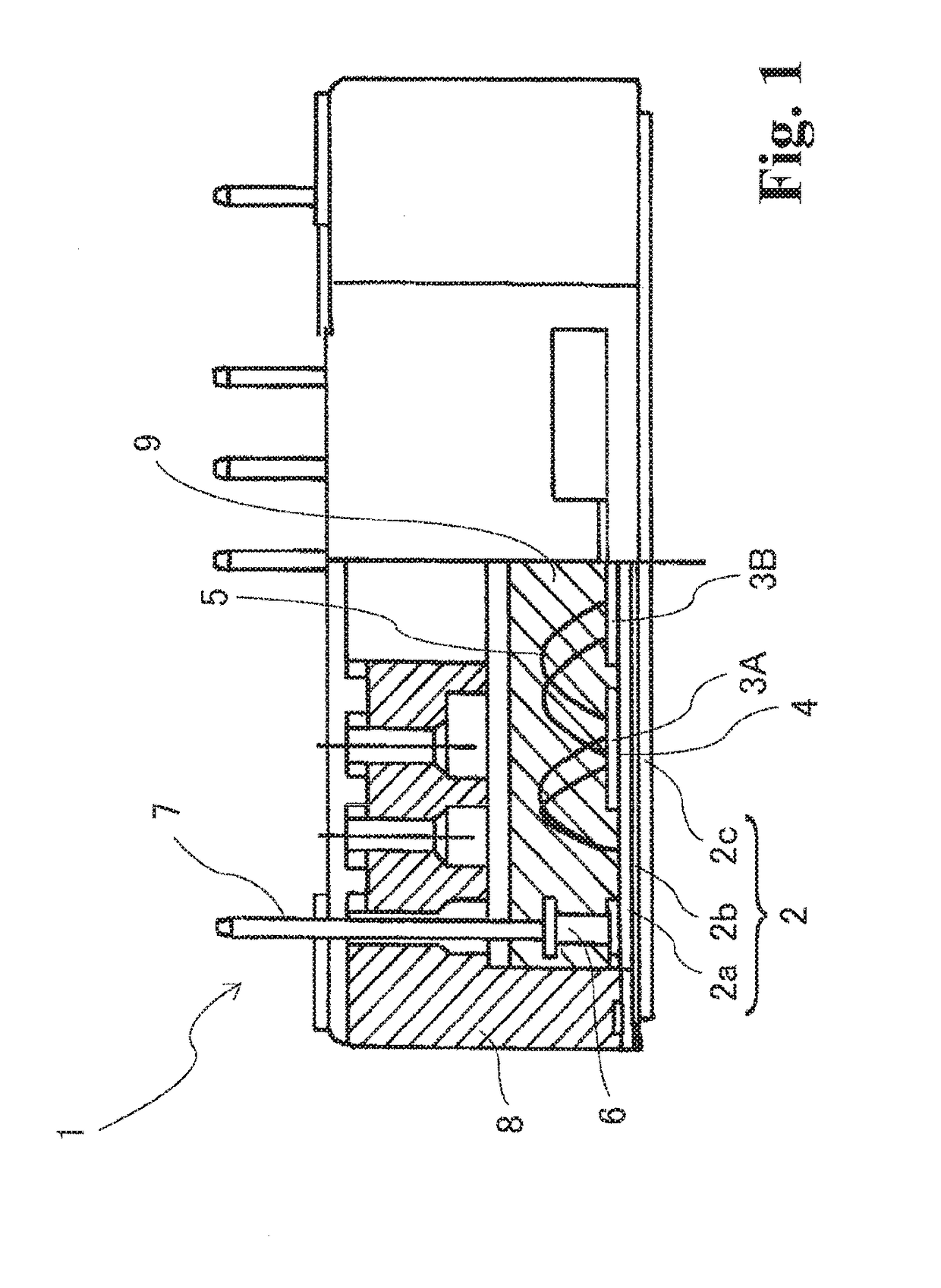
[0030]FIG. 1 is a front view in which a part is in cross-sectional view showing a semiconductor module 1 as an embodiment of a semiconductor device manufactured by a manufacturing method according to the invention. FIG. 2 is an enlarged cross-sectional view showing a principal part of the semiconductor module 1 shown in FIG. 1.

[0031]The semiconductor module 1, as is shown in FIG. 1 and FIG. 2, has at least one semiconductor chip, four semiconductor chips 3A, 3B, 3C, and 3D in the illustrated embodiment, as semiconductor elements mounted on an insulated circuit board 2. The semiconductor chips 3A, 3B, 3C, and 3D can be, for example, IGBT (Insulated Gate Bipolar Transistor) chips and FWD (Free Wheeling Diode) chips. The insulated circuit board 2 is formed of an insulating substrate 2a, a conductor pattern layer 2...


PUM

PropertyMeasurementUnit
Lengthaaaaaaaaaa
Lengthaaaaaaaaaa
Lengthaaaaaaaaaa

Abstract

A mounting jig for a semiconductor device includes an insulated circuit board positioning jig having a concave part in which an insulated circuit board is placed, a tubular contact element positioning jig disposed on an upper side of the insulated circuit board and having a plurality of positioning holes at predetermined positions to insert a plurality of tubular contact elements respectively, and a tubular contact element press-down jig having a flat plate and a plurality of projections extending from a lower surface of the flat plate. The plurality of projections includes a first length from the flat plate on a side closer to an outer circumference of the insulated circuit board, and a second length from the flat plate inside the outer circumference of the insulated circuit board. The first length is shorter than the second length.

Description

CROSS-REFERENCE TO RELATED APPLICATION[0001]This is a continuation-in-part application of U.S. patent application Ser. No. 14 / 923,941 filed on Oct. 27, 2015, which is a divisional application of U.S. patent application Ser. No. 14 / 204,455, filed on Mar. 11, 2014, which is based on, and claims priority to, Japanese Patent Application No. 2013-060987, filed on Mar. 22, 2013, contents of which are incorporated herein by reference.BACKGROUND OF INVENTIONField of the Invention[0002]The present invention relates to a mounting jig for mounting tubular contact elements with high accuracy onto a semiconductor device provided with the tubular contact elements.Background Art[0003]A power semiconductor module of semiconductor devices is generally a device, wherein a semiconductor chip such as an IGBT contained in a case is mounted on an insulated circuit board, provided with external terminals for connecting the semiconductor chip and the exterior of the case. In recent years, a technology of c...

Claims


Application Information

Patent Timeline
IPC IPC(8): H05K3/30H01L25/07H05K3/34H01L23/498H01L21/48H01L23/373H05K3/40
CPCH01L21/4853H01L2924/00H01L23/3735H01L25/072Y02P70/611Y02P70/613H01L23/49811Y10T29/41H05K3/301H05K3/303H05K3/341H05K3/4015H01L2924/13055H01L2224/48137H01L2224/48091H05K2203/0278H05K2201/1031H05K2201/10257H01L2924/00014H01L2924/1305Y10T29/532H01L24/29H01L24/45H01L2224/32225H01L2224/45124H01L2224/48227H01L2224/73265H01L2224/29101H01L24/48H01L24/49H01L24/73H01L2224/49109Y02P70/50H01L2924/014H01L2924/00012
Inventor MARUYAMA, RIKIHIROKAI, KENSHIKANZAWA, NOBUYUKISAWANO, MITSUTOSHI
Owner FUJI ELECTRIC CO LTD
Why Eureka
Try Eureka