
Method for fabricating conductive line

Active Publication Date: 2007-01-11
POWERCHIP SEMICON MFG CORP
View PDF2 Cites 1 Cited by
  • Summary
  • Abstract
  • Description
  • Claims
  • Application Information

AI Technical Summary

Benefits of technology

[0010] The object of the present invention is to provide a conductive line structure and a fabricating method thereof, suitable for fabricating a conductive line with smaller size and higher position accuracy.
[0023] Since the material of the first dielectric layer and the isolation structure of the present invention have different etching selectivity, the isolation structure can be used as a self-aligned mask when the first dielectric layer is patterned to form the opening exposing the first conductive layer. Moreover, since the material of the first dielectric layer and the material of the first conductive layer have different etching selectivity, the first conductive layer would not be damaged even if misalignment occurs, therefore the method of the present invention can increase the process margin. Meanwhile, since the fabricating method of the conductive line in the present invention can be further combined with the self-aligned shallow trench isolation (SASTI) process, the reliability of the whole structure can be further increased.
[0030] Since the fabricating method of the conductive line of the present invention can be combined with the self-aligned shallow trench isolation (SASTI) process, the reliability of the whole structure can be further increased. And since the material of the first dielectric layer and the material of the isolation structure of the present invention have different etching selectivity, the isolation structure can be used as a self-aligned mask when the first dielectric layer is patterned to form the opening that exposes the first conductive layer. Moreover, since the material of the first dielectric layer and the material of the first conductive layer have different etching selectivity, the first conductive layer would not be damaged even if misalignment occurs, therefore the process margin can be increased in the present invention.

Problems solved by technology

As a result, the difficulty of the fabricating process is increased.
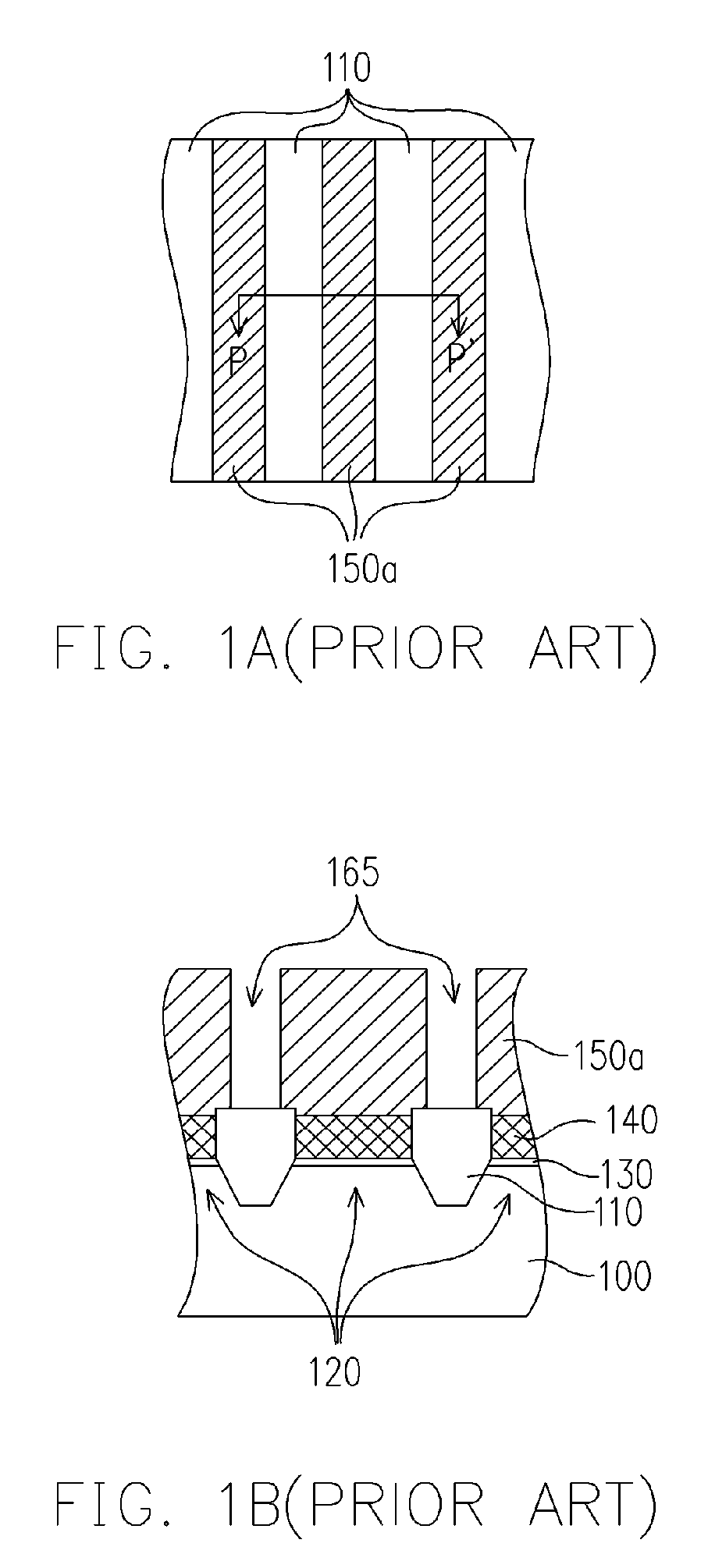
However, because of the limitation of the optical design rule of lithography, the method of fabricating the conductive line 150a using lithography and etching process can not be made with smaller size.
As a result, the electrical connection between devices are affected, therefore the devices can not work properly.

Method used


Image

  • Method for fabricating conductive line
  • Method for fabricating conductive line
  • Method for fabricating conductive line

Examples


first embodiment

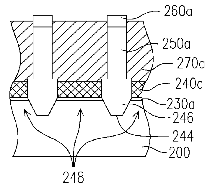
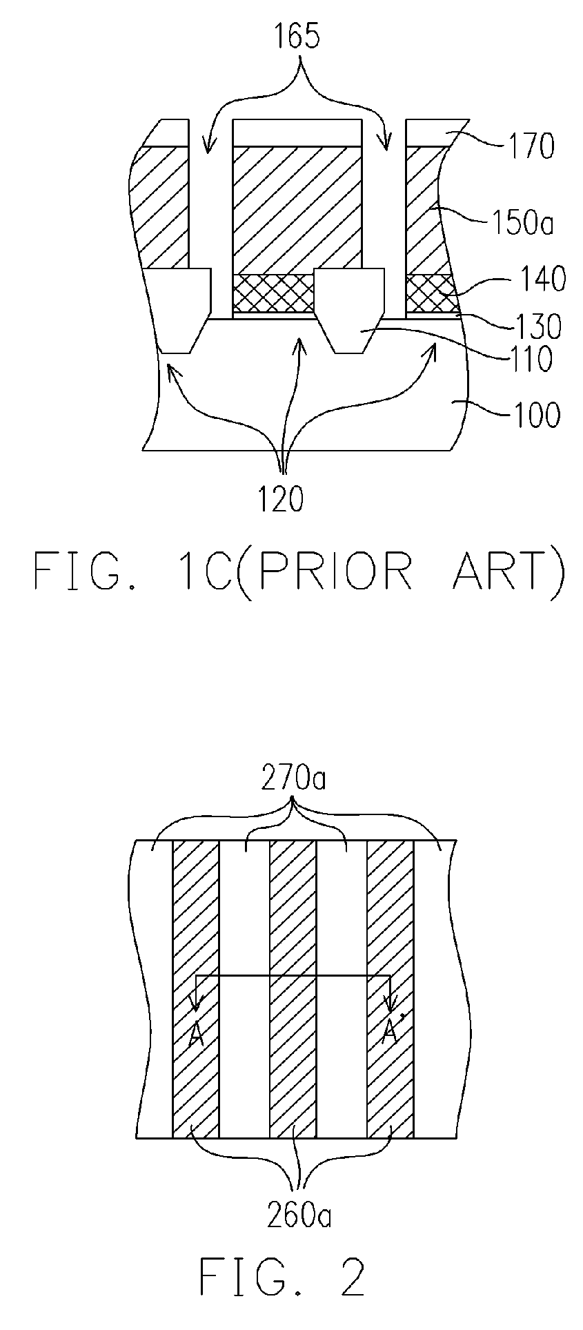
[0039]FIG. 2A˜FIG. 2G are schematic cross-sectional views along the line A-A′ in FIG. 2, illustrating the flowchart of fabricating the conductive line.

[0040] As shown in FIG. 2A, a substrate 200 is provided. On the substrate 200, an oxide layer 230, a conductive material layer 240 and a mask layer 242 are formed in sequence. The material of the oxide layer 230, for example, is silicon oxide. The material of conductive material layer 240, for example, is doped polysilicon or metal. And the material of mask layer 242, for example, is silicon nitride. The forming method of the oxide layer 230, for example, is a thermal oxidation process. The forming method of the conductive material layer 240 and the mask layer 242, for example, is a physical vapor deposition (PVD) or a chemical vapor deposition (CVD) process.

[0041] As shown in FIG. 2B, the mask layer 242, the conductive material layer 240 and the oxide layer 230 are patterned by using a dry etching process, for example, so as to for...

second embodiment

[0054]FIG. 3A is a schematic top view of an array with trench device, wherein the area circled by dotted line is where the trench device is located. FIG. 3B is a schematic cross-sectional view along line B-B′ in FIG. 3A, which schematically illustrates the cross-sectional view of the word line fabricating process in the fabricating process of the array with trench device. FIG. 3C is a schematic cross-sectional view along line C-C′ in FIG. 3A, which schematically illustrates the cross-sectional view of the word line fabricating process in the fabricating process of the array with trench device.

[0055] As shown in FIG. 3A to FIG. 3C, first, a substrate 320 is provided. A plurality of isolation structures 310 is formed in the substrate 320. And an active area 330 is defined between adjacent isolation structures 310. And the conductive layer 305 is formed in the active area 330. And a plurality of trench devices 300 are formed in the conductive layer. Wherein, the isolation structure 31...


PUM


Abstract

A method for fabricating a conductive line is provided. First, a substrate having at least two isolation structures already formed is provided. A first conductive layer is formed between every two isolation structures. Then, a dielectric layer is formed on the substrate. The dielectric layer is patterned to form an opening exposing the first conductive layer. After that, a second conductive layer is formed on the substrate. A portion of the second conductive layer outside the opening is removed to form a conductive line. As the size of the device is getting smaller, the size and the position accuracy of the conductive line would not be limited to the design rules of lithography if the present invention is applied. Therefore, a conductive line is formed to electrically connect semiconductor devices effectively.

Description

CROSS-REFERENCE TO RELATED APPLICATION [0001] This application claims the priority benefit of Taiwan application serial no. 94122796, filed on Jul. 6, 2005. All disclosure of the Taiwan application is incorporated herein by reference. BACKGROUND OF THE INVENTION [0002] 1. Field of Invention [0003] The present invention relates to a semiconductor device and the fabricating method of semiconductor device. More specifically, the present invention relates to the structure of a conductive line and the fabricating method of the same. [0004] 2. Description of Related Art [0005] Nowadays, integrated circuit technology is fast advancing, and device minimization and integration are an inevitable trend. While the device size is getting smaller, the size and line width of conductive lines for connecting devices are becoming smaller accordingly. As a result, the difficulty of the fabricating process is increased. [0006] Take the memory fabricated in the silicon wafer as an example, after forming...

Claims


Application Information

Patent Timeline
IPC IPC(8): H01L21/336
CPCH01L21/28273H01L29/42336H01L27/11521H01L27/115H01L29/40114H10B69/00H10B41/30
Inventor WANG, PIN-YAOLAI, LIANG-CHUANYANG, JENG-HUAN
Owner POWERCHIP SEMICON MFG CORP
Learn More