
Overvoltage protection device

a protection device and overvoltage protection technology, applied in the direction of coupling device connection, pulse technique, electronic switching, etc., to achieve the effect of prolonging the lifetime of the electronic apparatus and the electronic components

Active Publication Date: 2017-11-30
ALI (CHENGDU) CORP
View PDF1 Cites 1 Cited by
  • Summary
  • Abstract
  • Description
  • Claims
  • Application Information

AI Technical Summary

Benefits of technology

The invention is a device that prevents electronic devices from getting overvolted when using a USB and related components. It adds a delay and a switch to reduce the risk of damage. This results in a longer lifespan for the electronic devices.

Problems solved by technology

Therefore, it is an important issue to avoid the storage device and the electronic components to be under the overvoltage for long term, and meanwhile make the overvoltage protection circuit of the USB interface to be complied with the aforementioned situation.

Method used


Image

  • Overvoltage protection device
  • Overvoltage protection device
  • Overvoltage protection device

Examples


first embodiment

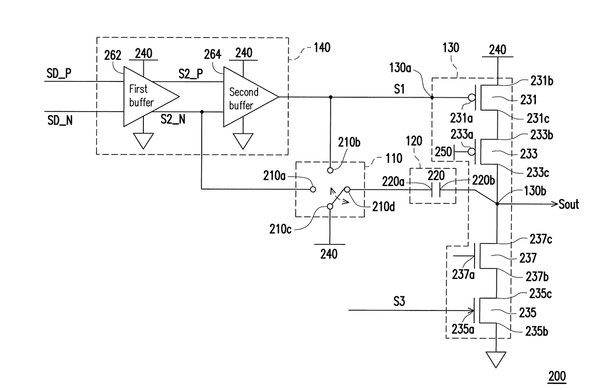
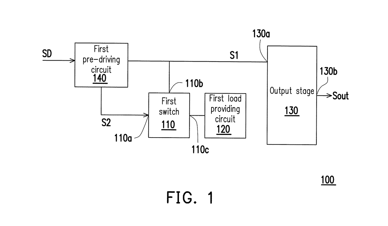
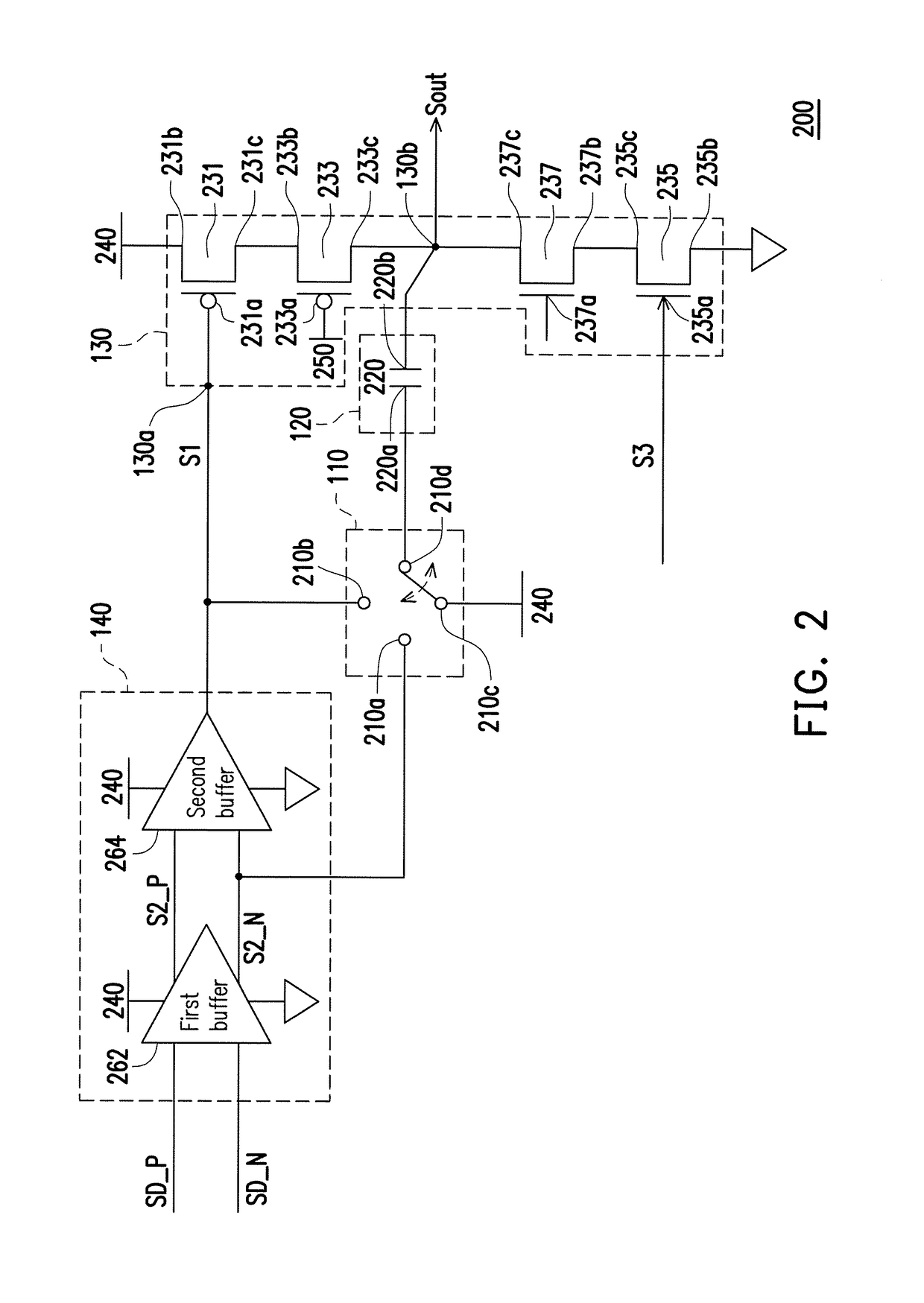
[0020]FIG. 1 is a block diagram of an overvoltage protection device 100 according to the invention. The overvoltage protection device 100 can be applied to an electronic apparatus having a universal serial bus (USB) interface, for example, a USB storage device, a mobile phone, etc. The USB storage device can be a flash drive, a hard disk drive, etc., that can use the USB interface. Referring to FIG. 1, the overvoltage protection device 100 of the present embodiment is mainly to transmit signals between different voltage levels. In the present embodiment, a voltage level of a data signal SD received by the overvoltage protection device 100 is between 0V and 1.8V, and a voltage level of an output signal Sout outputted by the overvoltage protection device 100 is between 0V and 3.3V. During a process of transmitting the data signal SD, the data signal SD can be boosted through a first pre-driving circuit 140, so as to generate a first signal S1 and a second signal S2, and an output stag...

second embodiment

[0045]FIG. 6 is a block diagram of an overvoltage protection device 500 according to the invention. The first switch 110, the first load providing circuit 120, the output stage 130 and the first pre-driving circuit 140 shown in FIG. 6 have the same functions and same circuit structures with that of FIG. 1, and details thereof are not repeated.

[0046]A main difference between the overvoltage protection devices of FIG. 6 and FIG. 1 is that the overvoltage protection device 600 further includes a second switch 650, a second load providing circuit 660 and a second pre-driving circuit 670. In the present embodiment, the second switch 650 has a circuit structure similar with that of the first switch 110, and the second load providing circuit 660 also has a circuit structure similar with that of the first load providing circuit 120. Those skilled in the art may learn enough instructions and recommendations for the second switch 650 and the second load providing circuit 660 from the related ...


PUM


Abstract

An overvoltage protection device including an output stage, a first switch and a first load providing circuit is provided. The output stage has a first input terminal to receive a first signal, and generates an output signal at an output terminal of the output stage according to the first signal. A first terminal of the first switch is coupled to the first input terminal of the output stage, and a control terminal of the first switch receives a second signal. The first signal is the delayed second signal. The first load providing circuit is coupled to a second terminal of the first switch. The first load providing circuit provides an impedance to the first input terminal when the first switch is turned on.

Description

CROSS-REFERENCE TO RELATED APPLICATION[0001]This application claims the priority benefit of China application serial no. 201610355692.0, filed on May 26, 2016. The entirety of the above-mentioned patent application is hereby incorporated by reference herein and made a part of this specification.BACKGROUND OF THE INVENTIONField of the Invention[0002]The invention relates to an overvoltage protection technique for electronic equipment, and particularly relates to an overvoltage protection device applied to a universal serial bus (USB) interface.Description of Related Art[0003]Universal serial bus (USB) interface supports functions of hot plug-in and plug-and-play. Since the advent of the USB interface, the USB interface has been widely applied to various electronic products, for example, USB storage devices, mobile phones, printers, personal computers, etc., and has become a mainstream interface for data exchange between various devices. Particularly, the USB storage device almost bec...

Claims


Application Information

Patent Timeline
Patent Type & Authority Applications(United States)
IPC IPC(8): H02H3/20H02H7/20
CPCH02H7/20H02H3/20H02M1/44H02M1/0003H03K19/00392H03K19/00346H03K17/166H01R13/00
Inventor CHENG, CHING-CHUNGLIN, KUO-KAI
Owner ALI (CHENGDU) CORP
Features
  • Generate Ideas
  • Intellectual Property
  • Life Sciences
  • Materials
  • Tech Scout
  • Unparalleled Data Quality
  • Higher Quality Content
  • 60% Fewer Hallucinations
Learn More