Organic light-emitting display device and method of manufacturing the same

a technology manufacturing methods, which is applied in the field of display technology, can solve the problems of difficult cost-effective manufacturing of organic light-emitting display devices at high volume with acceptable yield, and the applicability of organic light-emitting display devices is unequivocal, so as to reduce damage and facilitate the formation of an emission layer

Active Publication Date: 2017-12-21
SAMSUNG DISPLAY CO LTD
View PDF0 Cites 31 Cited by
  • Summary
  • Abstract
  • Description
  • Claims
  • Application Information

AI Technical Summary

Benefits of technology

[0006]One or more exemplary embodiments are directed towards organic light-emitting display devices and methods of manufacturing the same that may enable easier formation of an emission layer and an electrode of an organic light-emitting diode that may also protect (or at least reduce damage to) the organic light-emitting diode.

Problems solved by technology

The appeal of organic light-emitting display devices is unequivocal.
Cost-effective manufacturing of organic light-emitting display devices at high volume with acceptable yield is challenging.
It is noted, however, that such processes may cause, at least in part, a defect (e.g., a mask imprinting defect or phenomenon) to occur.

Method used


Image

  • Organic light-emitting display device and method of manufacturing the same
  • Organic light-emitting display device and method of manufacturing the same
  • Organic light-emitting display device and method of manufacturing the same

Examples


Embodiment Construction

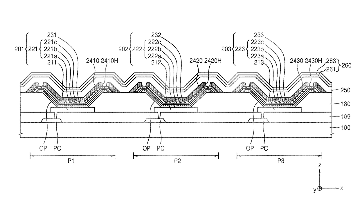
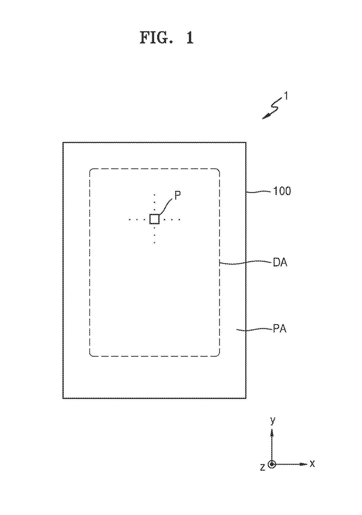
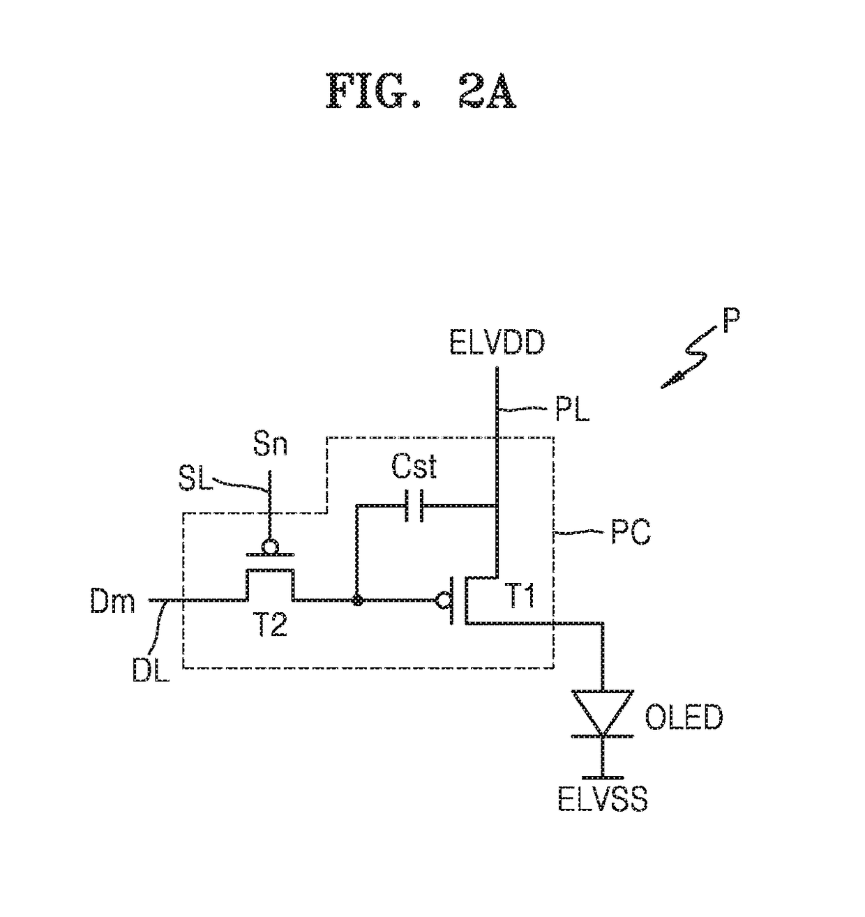
[0024]In the following description, for the purposes of explanation, numerous specific details are set forth in order to provide a thorough understanding of various exemplary embodiments. It is apparent, however, that various exemplary embodiments may be practiced without these specific details or with one or more equivalent arrangements. In other instances, well-known structures and devices are shown in block diagram form in order to avoid unnecessarily obscuring various exemplary embodiments.

[0025]Unless otherwise specified, the illustrated exemplary embodiments are to be understood as providing exemplary features of varying detail of various exemplary embodiments. Therefore, unless otherwise specified, the features, components, modules, layers, films, panels, regions, and / or aspects of the various illustrations may be otherwise combined, separated, interchanged, and / or rearranged without departing from the disclosed exemplary embodiments. Further, in the accompanying figures, the...


PUM


Abstract

An organic light-emitting display device includes: first and second pixel electrodes (PEs); a pixel-defining layer (PDL) disposed on the first and second PEs, the pixel-defining layer including first and second openings respectively exposing the first and second PEs; first and second intermediate layers (ILs) respectively disposed on the first and second PEs exposed via the first and second openings, each of the first and second ILs including an emission layer; first and second opposite electrodes (OEs) respectively disposed on the first and second ILs, the first and second OEs having an island-shaped pattern; first and second protective layers (PLs) respectively disposed on the first and second OEs, the first and second PLs having an island-shaped pattern; and a connection layer disposed on the first and second PLs, the connection layer electrically connecting the first and second OEs to one another.

Description

CROSS-REFERENCE TO RELATED APPLICATION[0001]This application claims priority from and the benefit of Korean Patent Application No. 10-2016-0075090, filed on Jun. 16, 2016, which is hereby incorporated by reference for all purposes as if fully set forth herein.BACKGROUNDField[0002]One or more exemplary embodiments relate to display technology, and, more particularly, to organic light-emitting display devices and methods of manufacturing the same.Discussion of the Background[0003]The appeal of organic light-emitting display devices is unequivocal. Not only do organic light-emitting display devices have a lightweight, slim profile, but they also exhibit advantages, such as wide viewing angles, fast response speeds, and low power consumption. Cost-effective manufacturing of organic light-emitting display devices at high volume with acceptable yield is challenging.[0004]Conventionally, formation of an organic light-emitting display device capable of producing a full range of colors via l...

Claims


Application Information

Patent Timeline
Patent Type & Authority Applications(United States)
IPC IPC(8): H01L51/52H01L51/00H01L51/56H01L51/50H01L27/32
CPCH01L51/5253H01L27/3246H01L51/5206H01L51/5221H01L51/5012H01L27/3276H01L2227/323H01L51/5056H01L51/5072H01L51/5092H01L51/56H01L51/0016H01L2251/301H01L51/5088H10K59/00H10K59/122H10K59/1213H10K59/131H10K50/805H10K50/844H10K71/00H10K50/82H10K50/8445H10K2102/101H10K59/1201H10K2102/351H10K50/11H10K50/15H10K50/16H10K50/17H10K50/81H10K50/171H10K71/221H10K2102/00
Inventor CHOUNG, JIYOUNGKWON, YOUNGGILLEE, DUCKJUNG
Owner SAMSUNG DISPLAY CO LTD
Why Eureka
Try Eureka