Vertical memory devices

a technology of vertical memory and memory device, which is applied in the direction of semiconductor devices, semiconductor/solid-state device details, electrical equipment, etc., can solve the problems of contact plugs in the peripheral region of vnand flash memory device that may not have a uniform density, electrical failure, etc., and achieve the effect of improving electrical characteristics

Active Publication Date: 2018-01-11
SAMSUNG ELECTRONICS CO LTD
View PDF4 Cites 10 Cited by
  • Summary
  • Abstract
  • Description
  • Claims
  • Application Information

AI Technical Summary

Benefits of technology

[0004]Example embodiments provide a vertical memory device including a contact plug having improved electrical characteristics.

Problems solved by technology

Contact plugs in a peripheral region of a VNAND flash memory device may not have a uniform density.
Contact plugs having a relatively low density may not be formed to contact a substrate or gate structure, or to have a size less than a desired size, which may generate an electrical failure.

Method used


Image

  • Vertical memory devices
  • Vertical memory devices
  • Vertical memory devices

Examples


Embodiment Construction

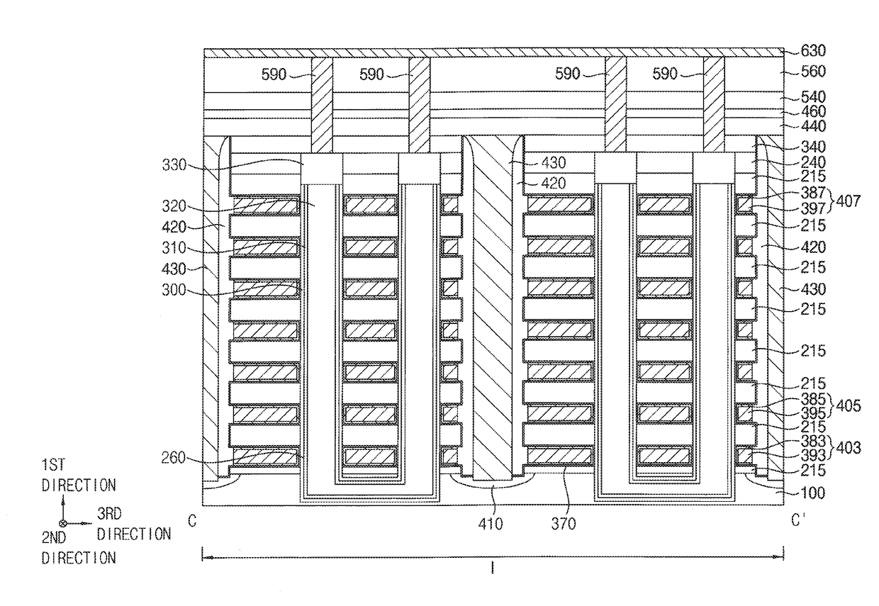
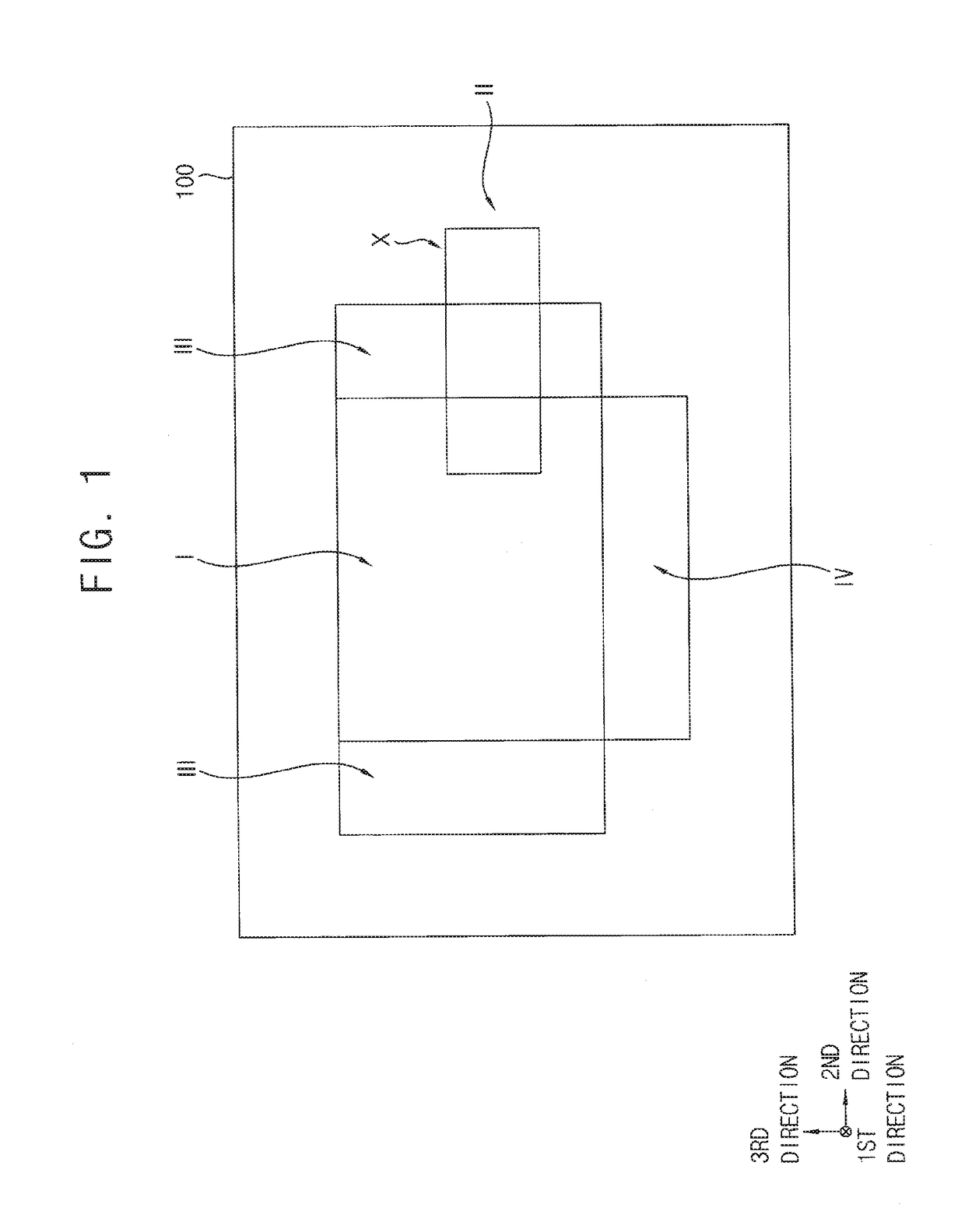
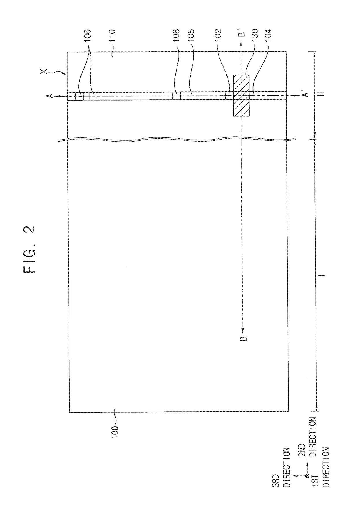
[0019]FIGS. 1 to 34 are cross-sectional views illustrating stages of a method of manufacturing a vertical memory device. Particularly, FIGS. 1-2, 5, 8, 10, 13, 18, 20, 22, 25, 28 and 31 are plan views, and FIGS. 3-4, 6-7, 9, 11-12, 14-17, 19, 21, 23-24, 26-27, 29-30 and 32-34 are cross-sectional views.

[0020]Each of the figures except for FIG. 1 shows a region X of FIG. 1. FIGS. 3, 23, 26, 29 and 32 are cross-sectional views taken along lines A-A′ of corresponding plan views, respectively, FIGS. 4, 6, 7, 16, 19, 24, 27, 30 and 33 are cross-sectional views taken along lines B-B′ of corresponding plan views, respectively, and FIGS. 9, 11, 12, 14, 15, 17, 18 and 34 are cross-sectional views taken along lines C-C′ of corresponding plan views. FIG. 12 is an enlarged cross-sectional view of a region Y of FIG. 11.

[0021]For purposes of illustration, a direction substantially perpendicular to an upper surface of a substrate is defined as a first direction, and two directions substantially par...


PUM


Abstract

A vertical memory device includes a substrate including a cell region and a peripheral circuit region, gate electrodes sequentially stacked on the cell region of the substrate in a vertical direction substantially perpendicular to an upper surface of the substrate, a channel on the cell region and extending through the gate electrodes in the vertical direction, a first lower contact plug on the peripheral circuit region and extending in the vertical direction, a second lower contact plug on the peripheral circuit region adjacent to the first lower contact plug and extending in the vertical direction, and a first upper wiring electrically connected to the first lower contact plug. The first upper wiring is configured to and apply an electrical signal to the first lower contact plug. The second lower contact plug is not electrically connected to an upper wiring configured to apply an electrical signal.

Description

CROSS-REFERENCE TO RELATED APPLICATIONS[0001]This application claims priority under 35 U.S.C. §119 to Korean Patent Application No. 10-2016-0087722 filed on Jul. 11, 2016 in the Korean Intellectual Property Office (KIPO), the contents of which are incorporated by reference herein in their entirety.BACKGROUND1. Field[0002]Inventive concepts generally relate to a vertical memory device, and more particularly, inventive concepts relate to a vertical non-volatile memory device having a contact plug.2. Description of Related Art[0003]Contact plugs in a peripheral region of a VNAND flash memory device may not have a uniform density. Contact plugs having a relatively low density may not be formed to contact a substrate or gate structure, or to have a size less than a desired size, which may generate an electrical failure.SUMMARY[0004]Example embodiments provide a vertical memory device including a contact plug having improved electrical characteristics.[0005]According to some example embod...

Claims


Application Information

Patent Timeline
Patent Type & Authority Applications(United States)
IPC IPC(8): H01L23/528
CPCH01L27/11582H01L27/11556H01L23/5283H10B43/10H10B43/50H10B43/35H10B43/27H01L21/76802H10B41/40H10B41/20H10B43/40H10B43/20H10B41/27
Inventor KIM, KYOUNG-HOONKIM, HONG-SOOLEE, JU-YEON
Owner SAMSUNG ELECTRONICS CO LTD
Why Eureka
Try Eureka