

Method and Device for Inspecting an Optoelectronic Component
- Summary
- Abstract
- Description
- Claims
- Application Information
AI Technical Summary
Benefits of technology
Problems solved by technology
Method used
Image

Examples
first embodiment
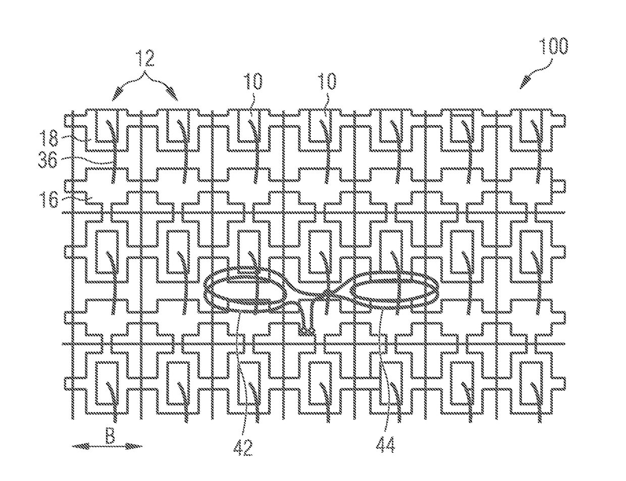
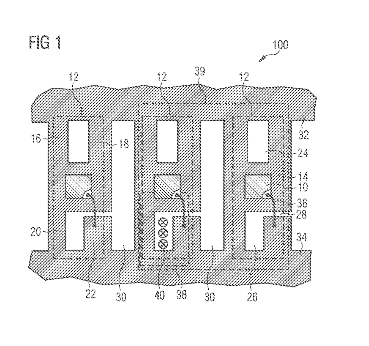
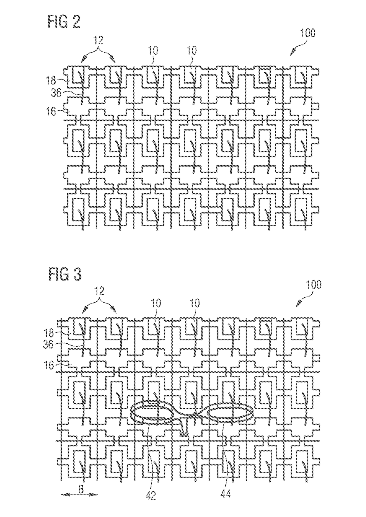
[0061]FIG. 3 schematically shows a method for inspecting an optoelectronic component. It shows the connection board 100 illustrated in FIG. 2, above or below which a double coil is arranged, which comprises a first coil 42 and a second coil 44. The arrangement of the double coil 42, 44 is illustrated only in diagrammatic form. The double coil 42, 44 generates a temporally variable electromagnetic alternating field, which induces an electrical alternating voltage in a local region of the connection board 100 and thus excites an electromagnetic resonant circuit. The excitation of the electromagnetic resonant circuit here takes place in a manner similar to that already explained in association with FIG. 1. The first coil 42 and the second coil 44 are spaced apart from one another laterally, more specifically in a direction parallel to a main extension plane of the connection board 100 and perpendicular to the central axes or axes of symmetry of the two coils 42, 44. A distance between ...
second embodiment
[0064]FIG. 4 schematically shows a method for inspecting an optoelectronic component. In this embodiment, in addition to the coils 42, 44, electrical contacts 46, e.g., needle contacts or pogo pins, are provided, which are arranged such that short circuit paths are generated on the connection board 100. As a result, defined current paths are obtained and, e.g., undesired leakage current paths are reduced.
[0065]FIGS. 5 and 6 schematically show the portions of the magnetic field 43, 45 generated by the two coils 42, 44. The two coils 42, 44 are wound in opposite directions, such that the magnetic field 43 inside the first coil 42 is always directed antiparallel to the magnetic field 45 inside the second coil 44. As a result, two voltages 48, 50 having opposite rotational directions are induced by the two coils on the connection board, which voltages add in a region in the center between the two coils 42, 44. An electromagnetic resonant circuit is or electromagnetic resonant circuits a...
third embodiment
[0066]FIG. 7 shows a diagram of a flat coil 52 for use in a method for inspecting an optoelectronic component. The flat coil 52 is formed by a wound metal wire, has the shape of an Archimedean spiral and in the present case has four windings. An even better field convergence can be obtained by means of a higher number of windings. Alternatively or additionally, an increase in the generated field strength can also be achieved by the arrangement of a ferrite core 54 in the center of the flat coil 52 (see FIG. 8).
[0067]FIGS. 9 to 11 show embodiments in which the flat coil 52 is formed by a patterned circuit board. An arrangement of this type can be produced in particular by photochemical etching of a circuit board. Depending on the part size and available space, the use of a ferromagnetic element for additional field convergence is also feasible.
[0068]FIGS. 10 and 11 show special embodiments in which selective excitation of one or a few optoelectronic components on the connection board...
PUM
 Abstract
Description
Claims
Application Information