Large power LED double-layer package structure

A packaging structure, high-power technology, applied in semiconductor devices, electrical components, circuits, etc., can solve the problems of reducing the light extraction efficiency of the package, the quantum efficiency of the phosphor powder, and affecting the lumen efficiency of the package, so as to improve the utilization rate of the light source and solve the Reduced quantum efficiency and good heat dissipation

Inactive Publication Date: 2018-04-20
XIAN CREATION KEJI CO LTD
View PDF6 Cites 0 Cited by
  • Summary
  • Abstract
  • Description
  • Claims
  • Application Information

AI Technical Summary

Problems solved by technology

Since the chip absorbs the backscattered light, this direct coating method will reduce the light extraction efficiency of the package
In addition, if the phosphor is directly coated on the chip, the high temperature generated by the chip will significantly reduce the quantum efficiency of the phosphor, which will seriously affect the lumen efficiency of the package.

Method used


Image

  • Large power LED double-layer package structure
  • Large power LED double-layer package structure

Examples


Embodiment 1

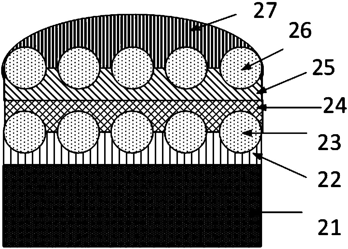
[0029] figure 1 A schematic diagram of a high-power LED double-layer package structure provided for the embodiment of the present invention, including: a heat dissipation substrate 21, a first package layer 22, a second package layer 24, a third package layer 25, a fourth package layer 27, several A spherical lens 23, several second spherical lenses 26;

[0030] The first encapsulation layer 22 is located on the heat dissipation substrate 21, at least a part of the first spherical lens 23 is embedded in the first encapsulation layer 22, and the second encapsulation layer 24 is located where the spherical lens 23 is not embedded. part and above the first encapsulation layer 22;

[0031] The third encapsulation layer 25 is located on the second encapsulation layer 24, at least a part of the second spherical lens 26 is embedded in the third encapsulation layer 25, and the fourth encapsulation layer 27 is located on the second spherical lens. The lens 26 is on the non-embedded p...


PUM

PropertyMeasurementUnit
Diameteraaaaaaaaaa

Abstract

The invention discloses a large power LED double-layer package structure. The structure comprises a radiating substrate (21), a first package layer (22), a second package layer (24), and a plurality of spherical lenses (23); the first package layer (22) is coated on the radiating substrate (21), at least a part of the spherical lens (23) is embedded in the first package layer (22), and the secondpackage layer (24) is coated on the unembedded part of the spherical lens (23). By adopting the spherical lenses, the large power LED double-layer package structure solves the technical problem that the light source illuminating brightness is not enough in concentration, the secondary shaping is unnecessary, the structure is simple, and the production cost is reduced. Furthermore, an operation ofsmearing fluorescent powder on a chip is unnecessary in comparison with the prior art, the problem that the brightness is reduced since the high temperature causes the quantum efficiency reduction ofthe fluorescent powder is solved.

Description

technical field [0001] The invention belongs to the field of semiconductor packaging, in particular to a high-power LED double-layer packaging structure. Background technique [0002] LED has the characteristics of long life, high luminous efficiency, good color rendering, safety and reliability, rich colors and easy maintenance. At present, LEDs mostly use GaN-based blue light wicks plus yellow fluorescent light to generate white light to achieve lighting. [0003] However, the prior art has the following drawbacks. [0004] 1. Since the light emitted by the LED light source is generally distributed in a divergent manner, that is, the Lambertian distribution, this causes the illumination brightness of the light source to be insufficiently concentrated. The existing silicone lens generally needs to be reshaped by an external lens to meet the lighting requirements of specific occasions. The structure is complicated and the production cost is higher. [0005] 2. In the exis...

Claims


Application Information

Patent Timeline
IPC IPC(8): H01L33/50H01L33/54H01L33/56H01L33/58H01L33/64
CPCH01L33/507H01L33/54H01L33/56H01L33/58H01L33/641H01L33/642
Inventor 尹晓雪
Owner XIAN CREATION KEJI CO LTD
Why Eureka
Try Eureka