Method of detecting liquid crystal display panel yield

a liquid crystal display panel and yield technology, applied in non-linear optics, instruments, optics, etc., can solve the problems of shortening the required time, affecting the detection efficiency, and the quality and yield condition of the liquid crystal display panel cannot be quickly responded to, so as to achieve rapid response, promote detection yield, and save time

Inactive Publication Date: 2018-02-15
WUHAN CHINA STAR OPTOELECTRONICS TECH CO LTD
View PDF2 Cites 0 Cited by
  • Summary
  • Abstract
  • Description
  • Claims
  • Application Information

AI Technical Summary

Benefits of technology

[0025]The benefits of the present invention are: the present invention provides a method of detecting a liquid crystal display panel yield, and the signal lines of the same function in each liquid crystal display panel are coupled to one wire, and the wire extends to a periphery of the liquid crystal display mainboard to form mainboard assembled wires corresponding to all the liquid crystal display panels, and the respective mainboard assembled wires are employed to drive the liquid crystal display mainboard to detect all the liquid crystal display panels at the same time. In comparison with prior art, the processes of the first cut, the thinning, the second cut and the lamination before the detection can be decreased. Thus, the time can be saved to rapidly respond the quality and the yield condition of the liquid crystal display panel for promoting the detection yield.

Problems solved by technology

The processes are more, and the required time is longer, and the detection efficiency is lower, and the quality and the yield condition of the liquid crystal display panel cannot be rapidly responded.

Method used


Image

  • Method of detecting liquid crystal display panel yield
  • Method of detecting liquid crystal display panel yield
  • Method of detecting liquid crystal display panel yield

Examples


Embodiment Construction

[0030]For better explaining the technical solution and the effect of the present invention, the present invention will be further described in detail with the accompanying drawings and the specific embodiments.

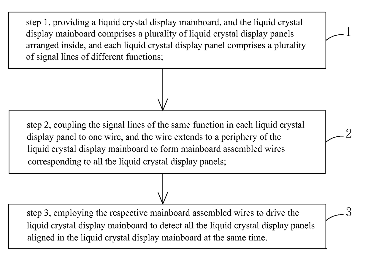
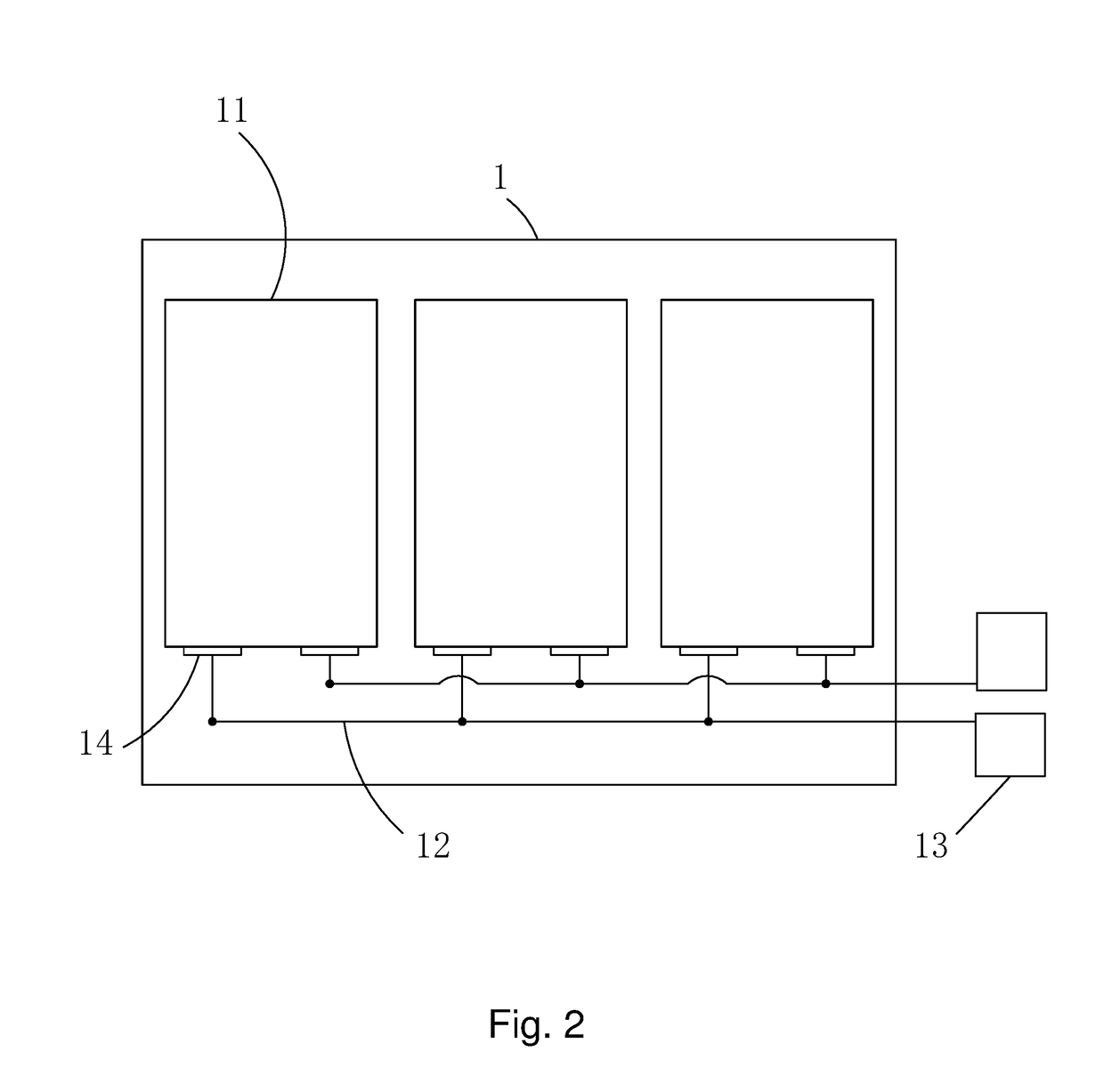
[0031]Please refer to FIG. 1 and FIG. 2 at the same time, the present invention provides a method of detecting a liquid crystal display panel yield, comprising steps of:

[0032]step 1, providing a liquid crystal display mainboard 1, and the liquid crystal display mainboard 1 comprises a plurality of liquid crystal display panels 11 arranged inside, and each liquid crystal display panel 11 comprises a plurality of signal lines of different functions.

[0033]Specifically, the plurality of liquid crystal display panels 11 are aligned in array in the liquid crystal display mainboard 1. Two adjacent liquid crystal display panels 11 are mutually spaced so that the unique liquid crystal display panel with the specific dimension can be obtained after ultimately cutting the liquid crystal ...


PUM

PropertyMeasurementUnit
timeaaaaaaaaaa
driving voltagesaaaaaaaaaa
voltageaaaaaaaaaa

Abstract

The present invention provides a method of detecting a liquid crystal display panel yield, and the signal lines of the same function in each liquid crystal display panel (11) are coupled to one wire (12), and the wire (12) extends to a periphery of the liquid crystal display mainboard (1) to form mainboard assembled wires (13) corresponding to all the liquid crystal display panels (11), and the respective mainboard assembled wires (13) are employed to drive the liquid crystal display mainboard (1) to detect all the liquid crystal display panels (11) at the same time. In comparison with prior art, the processes of the first cut, the thinning, the second cut and the lamination before the detection can be decreased. Thus, the time can be saved to rapidly respond the quality and the yield condition of the liquid crystal display panel for promoting the detection yield.

Description

FIELD OF THE INVENTION[0001]The present invention relates to a display technology field, and more particularly to a method of detecting a liquid crystal display panel yield.BACKGROUND OF THE INVENTION[0002]The LCD (Liquid Crystal Display) possesses many advantages of being ultra thin, power saved and radiation free. It has been widely utilized in, such as LCD TVs, mobile phones, Personal Digital Assistant (PDA), digital cameras, laptop screens or notebook screens, and dominates the flat panel display field.[0003]Most of the liquid crystal displays on the present market are backlight type liquid crystal displays, which comprise a liquid crystal display panel and a backlight module. The working principle of the liquid crystal display panel is that the Liquid Crystal is injected between the Thin Film Transistor Array Substrate (TFT array substrate) and the Color Filter (CF). The light of backlight module is refracted to generate images by applying driving voltages to the two substrates...

Claims


Application Information

Patent Timeline
Patent Type & Authority Applications(United States)
IPC IPC(8): G02F1/1362G02F1/1335
CPCG02F1/136286G02F1/133514G02F2001/1635G02F1/1309G02F1/133351G02F1/136254
Inventor YANG, SHAOFU
Owner WUHAN CHINA STAR OPTOELECTRONICS TECH CO LTD
Why Eureka
Try Eureka