Method and apparatus for contact image sensing

a contact image and sensor technology, applied in the field of image sensors, can solve the problems of blurred or vague images, inability to accurately detect the quality of inked images, and excessive time-consuming finger printing using the traditional method of inking a finger and applying the inked finger to paper, and achieve the effect of high resolution

Active Publication Date: 2018-03-15
DIGILENS
View PDF2 Cites 51 Cited by
  • Summary
  • Abstract
  • Description
  • Claims
  • Application Information

AI Technical Summary

Benefits of technology

[0007]It is an object of the present invention to provide a portable, high resolution, lightweight biometeric contact image scanner.

Problems solved by technology

Fingerprinting using the traditional method of inking a finger and applying the inked finger to paper can be extremely time-consuming.
Problems can arise due to the quality of inked images.
For example, applying too much or too little ink may result in blurred or vague images.
Further, the process of scanning an inked image can be time-consuming.
While the fingerprinting systems disclosed in the foregoing patents are capable of providing optical or optical and mechanical fingerprint images, such systems are only suitable for use at a central location such as a police station.
Such a system is clearly not ideal for law enforcement and security applications where there is the need to perform an immediate identity and background check on an individual while in the field.
In general, current contact image sensor technology tend to be bulky, low in resolution and unsuitable for operation in the field.

Method used


Image

  • Method and apparatus for contact image sensing
  • Method and apparatus for contact image sensing
  • Method and apparatus for contact image sensing

Examples


Embodiment Construction

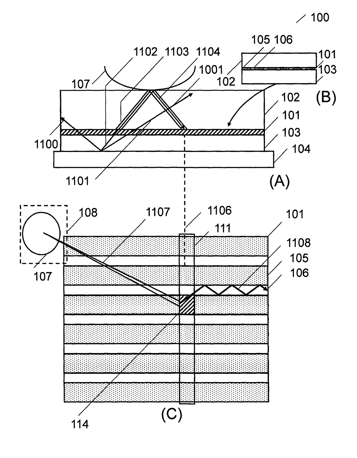
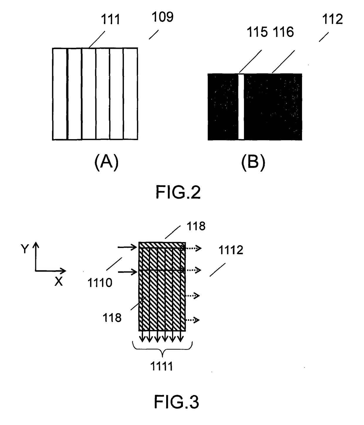
[0066]It will be apparent to those skilled in the art that the present invention may be practiced with some or all of the present invention as disclosed in the following description. For the purposes of explaining the invention well-known features of optical technology known to those skilled in the art of optical design and visual displays have been omitted or simplified in order not to obscure the basic principles of the invention. Unless otherwise stated the term “on-axis” in relation to a ray or a beam direction refers to propagation parallel to an axis normal to the surfaces of the optical components described in relation to the invention. In the following description the terms light, ray, beam and direction may be used interchangeably and in association with each other to indicate the direction of propagation of light energy along rectilinear trajectories. Parts of the following description will be presented using terminology commonly employed by those skilled in the art of opt...


PUM

PropertyMeasurementUnit
widthaaaaaaaaaa
angleaaaaaaaaaa
thicknessaaaaaaaaaa

Abstract

A contact image sensor having a waveguiding structure for propagating light in a first direction including, in series, a first clad medium, a first core, a switchable grating clad, a second core, and a second clad medium sandwiched by transparent substrates, patterned parallel electrode elements orthogonally traversing the waveguides, a light source, a platen and a detector. Switchable grating regions overlapped by a first voltage-addressed electrode element diffract TIR light from the first core towards the platen. Switchable grating region overlapped by a second voltage-addressed electrode element diffract TIR light reflected from the platen into a TIR path within the second core.

Description

PRIORITY CLAIM[0001]This application claims priority from U.S. Provisional Application Ser. No.: 62 / 178,041 entitled METHOD AND APPARATUS FOR CONTACT IMAGE SENSING filed on 31 Mar. 2015, which is hereby incorporated by reference in its entiretyCROSS REFERENCE TO RELATED APPLICATIONS[0002]The following patent applications are hereby incorporated by reference herein in their entireties: PCT Application No.: PCT / GB2012 / 000680 entitled IMPROVEMENTS TO HOLOGRAPHIC POLYMER DISPERSED LIQUID CRYSTAL MATERIALS AND DEVICES with filing date 7 Jan. 2013; PCT Application No.: PCT / GB2012 / 000729 entitled METHOD AND APPARATUS FOR SWITCHING ELECTRO OPTICAL ARRAYS with filing date 6 Sep. 2012; PCT Application No.: PCT / GB2013 / 000005 entitled CONTACT IMAGE SENSOR USING SWITCHABLE BRAGG GRATINGS with filing date 7 Jan. 2013; U.S. Pat. No.: 8,354,640 entitled OPTICALLY-BASED PLANAR SCANNER with issue date 15 Jan. 2013; PCT Application No.: PCT / GB2014 / 000295 entitled METHOD AND APPARATUS FOR CONTACT IMAGE...

Claims


Application Information

Patent Timeline
Patent Type & Authority Applications(United States)
IPC IPC(8): G02F1/13G02B26/08G02B27/42G02F1/29
CPCG02F1/1326G02B26/0808G02B27/4272G02F1/29G02B5/1828
Inventor POPOVICH, MILAN MOMCILOWALDERN, JONATHAN DAVIDGRANT, ALASTAIR JOHN
Owner DIGILENS
Why Eureka
Try Eureka