Check patentability & draft patents in minutes with Patsnap Eureka AI!

Semiconductor device

a technology of semiconductor devices and semiconductors, applied in semiconductor devices, semiconductor/solid-state device details, electrical apparatus, etc., can solve problems such as difficulty in ensuring structural stability

Inactive Publication Date: 2018-04-12
SK HYNIX INC
View PDF9 Cites 7 Cited by
  • Summary
  • Abstract
  • Description
  • Claims
  • Application Information

AI Technical Summary

Benefits of technology

This configuration improves the structural stability of the stacked body, reducing distortion and collapse risks, thereby enhancing the integration and performance of three-dimensional semiconductor memory devices.

Problems solved by technology

When the height of the stacked body increases, it may be difficult to ensure the structural stability.

Method used


Image

  • Semiconductor device
  • Semiconductor device
  • Semiconductor device

Examples


Embodiment Construction

[0015]Hereinafter, examples of embodiments will now be described more fully hereinafter with reference to the accompanying drawings; however, they may be embodied in different forms and should not be construed as limited to the embodiments set forth herein. Rather, these embodiments are provided so that this disclosure will be thorough and complete, and will fully convey the scope of the examples of embodiments to those skilled in the art.

[0016]Embodiments of the present disclosure may provide for a semiconductor device capable of enhancing structural stability of a stacked body.

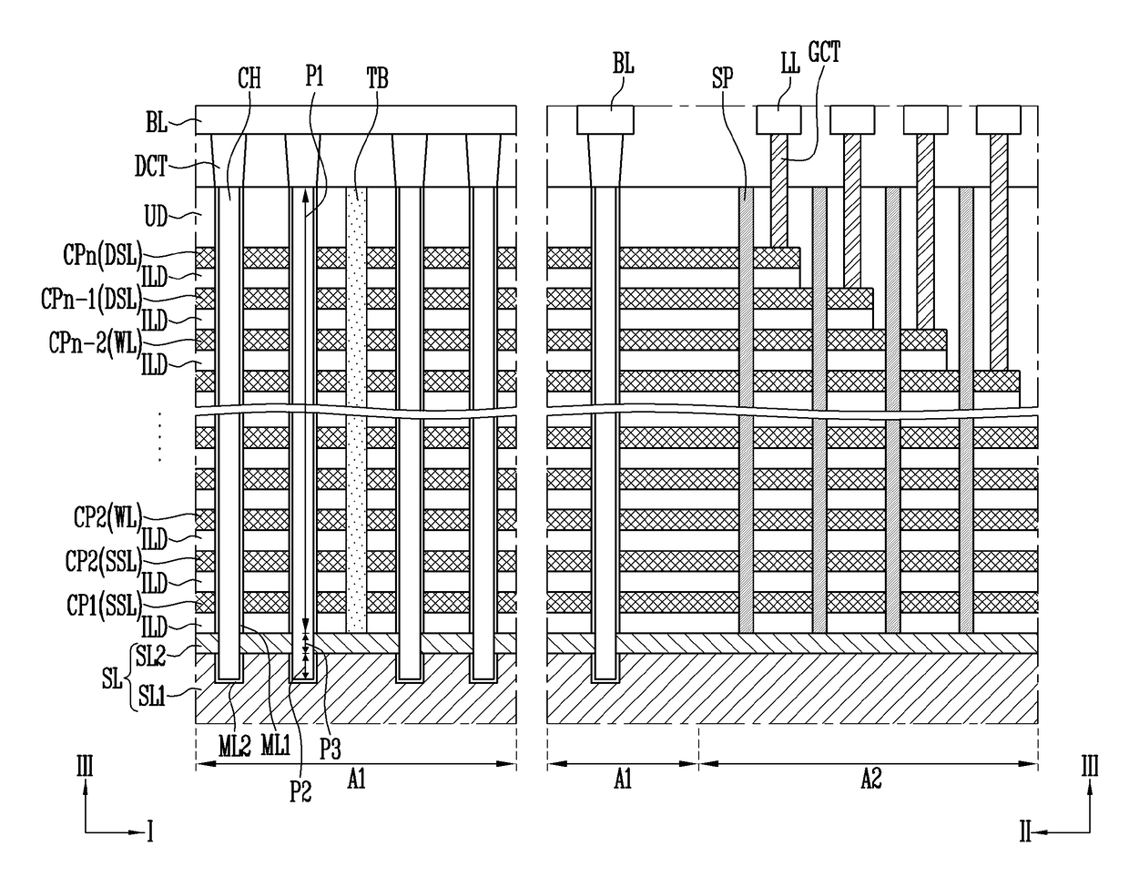
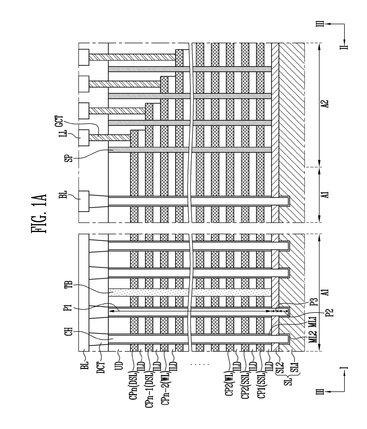
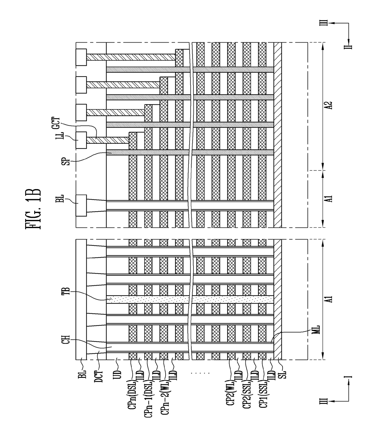
[0017]FIGS. 1A to 1C are cross-sectional views illustrating a semiconductor device according to embodiments of the present disclosure. FIGS. 1A to 1C each illustrate a cross-section taken along a first direction I and a cross-section taken along a second direction II of the semiconductor device. The first direction I may be an extension direction of a bit line BL and the second direction II may intersect the...


PUM


Abstract

A semiconductor device may be provided. The semiconductor device may include conductive patterns surrounding a channel film. The conductive patterns may be stacked and spaced apart from one another. The semiconductor device may include a gate contact plug coupled to one of the conductive patterns. The semiconductor device may include support pillars penetrating the conductive patterns in a periphery of the gate contact plug.

Description

CROSS-REFERENCE TO RELATED APPLICATION[0001]The present application is a divisional application of U.S. application Ser. No. 15 / 458,330, filed on Mar. 14, 2017, and claims priority under 35 U.S.C. § 119(a) to Korean patent application number 10-2016-0113290 filed on Sep. 2, 2016 in the Korean Intellectual Property Office, the entire disclosure of which is incorporated herein by reference.BACKGROUND1. Technical Field[0002]Various embodiments of the present disclosure may generally relate to a semiconductor device, and more particularly to, a semiconductor device including a stacked body.2. Related Art[0003]To improve the degree of integration of semiconductor devices, the semiconductor device may be formed in various structures. For example, a three-dimensional semiconductor memory device may include memory cells arranged in a three-dimensional structure. Thus, the three-dimensional semiconductor memory device may increase the number of memory cells arranged in a unit area of a subst...

Claims


Application Information

Patent Timeline
Patent Type & Authority Applications(United States)
IPC IPC(8): H01L23/528H01L27/11582H01L23/522H01L27/1157H10B69/00H10B43/27H10B43/35
CPCH01L27/11582H01L23/5226H01L27/1157H01L23/528H01L29/407H01L21/76898H10B41/50H10B41/35H10B43/50H10B41/27H10B43/35H10B43/27
Inventor KIM, DO YOUNYUNE, HYOUNG SOON
Owner SK HYNIX INC
Features
  • R&D
  • Intellectual Property
  • Life Sciences
  • Materials
  • Tech Scout
  • Unparalleled Data Quality
  • Higher Quality Content
  • 60% Fewer Hallucinations
Learn More