Fin-fet devices and fabrication methods thereof

Active Publication Date: 2018-04-19
SEMICON MFG INT (SHANGHAI) CORP +1
View PDF4 Cites 0 Cited by
  • Summary
  • Abstract
  • Description
  • Claims
  • Application Information

AI Technical Summary

Benefits of technology

The patent text describes a process for making a fin structure on a substrate. The width of the fin structure decreases gradually from the bottom to the top, due to the characteristics of the etching process. This is caused by the regathering of etching byproducts at the bottom of the fin structure. The text suggests that this variation in width could be controlled by adjusting the etching process.

Problems solved by technology

As such, the controllability of the gate electrode on the channel may be degraded and the gate voltage may not be able to pinch off the channel.
As a result, the subthreshold leakage phenomenon, e.g. the short-channel effect (SCE), may easily occur.

Method used


Image

  • Fin-fet devices and fabrication methods thereof
  • Fin-fet devices and fabrication methods thereof
  • Fin-fet devices and fabrication methods thereof

Examples


Embodiment Construction

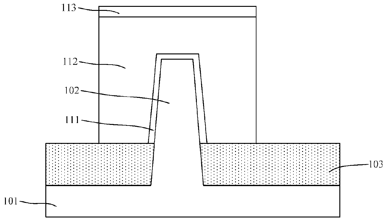
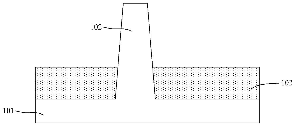
[0014]Reference will now be made in detail to exemplary embodiments of the invention, which are illustrated in the accompanying drawings. Wherever possible, the same reference numbers will be used throughout the drawings to refer to the same or like parts.

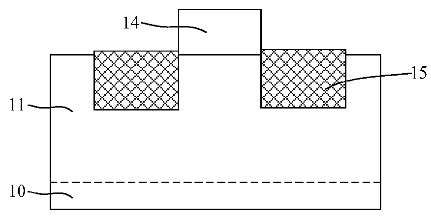
[0015]FIG. 1 illustrates schematic cross-section views of a Fin-FET device. Specifically, the left panel of FIG. 1 illustrates a schematic cross-section view of the Fin-FET device along a direction perpendicular to the length direction of the fin structure in the Fin-FET device, and the right panel of FIG. 1 illustrates a schematic cross-section view of the Fin-FET device along the length direction of the fin structure.

[0016]Referring to FIG. 1, the Fin-FET includes a substrate 10, a fin structure 11 protruding from the substrate 10, and an isolation structure 13 formed on the substrate 10. The isolation structure 13 covers a portion of each sidewall surface of the fin structure 11, and the top surface of the isolation structure 13...


PUM


Abstract

A method for fabricating a Fin-FET device includes providing a base structure and a plurality of fin structures protruding from the base structure. Along a direction perpendicular to the surface of the base structure and from the bottom to the top of each fin structure, the width of the fin structure perpendicular to the length direction of the fin structure decreases. The method further includes forming a gate structure on the base structure across each fin structure and covering a portion of top and sidewall surfaces of the fin structure, and removing a portion of the fin structure on each side of the gate structure to form a trench in the fin structure. Along the length direction of the fin structure, the bottom width of the trench is smaller than the top width of the trench. The method also includes filling each trench with a doped source / drain epitaxial layer.

Description

CROSS-REFERENCES TO RELATED APPLICATIONS[0001]This application claims the priority of Chinese Patent Application No. CN201610908755.0, filed on Oct. 18, 2016, the entire content of which is incorporated herein by reference.FIELD OF THE DISCLOSURE[0002]The present disclosure generally relates to the field of semiconductor fabrication technology and, more particularly, relates to fin field-effect transistors and fabrication methods thereof.BACKGROUND[0003]With continuous development of semiconductor technology, the development of the semiconductor process node demonstrates a growing trend to fall off the Moore's law. In order to accommodate the decrease of the process node, the channel length in metal-oxide-semiconductor field-effect transistor (MOSFET) has to be reduced. Reducing the channel length may benefit the increase of transistor density on the semiconductor chip and may also be conducive to improving the switching speed of the MOSFET.[0004]However, as the channel length in de...

Claims


Application Information

Patent Timeline
IPC IPC(8): H01L21/8238H01L27/092H01L21/265H01L21/324
CPCH01L21/823878H01L21/823814H01L27/0924H01L21/823821H01L21/26513H01L21/324H01L29/66795H01L29/7853H01L29/7848
Inventor LI, YONG
Owner SEMICON MFG INT (SHANGHAI) CORP
Why Eureka
Try Eureka