Circuit substrate and display device

Active Publication Date: 2021-07-22
SHARP KK
View PDF3 Cites 1 Cited by
  • Summary
  • Abstract
  • Description
  • Claims
  • Application Information

AI Technical Summary

Benefits of technology

The patent describes a way to make frames narrower.

Problems solved by technology

Thus, it has been difficult to keep the frame width of element substrates small.

Method used


Image

  • Circuit substrate and display device
  • Circuit substrate and display device
  • Circuit substrate and display device

Examples


first embodiment

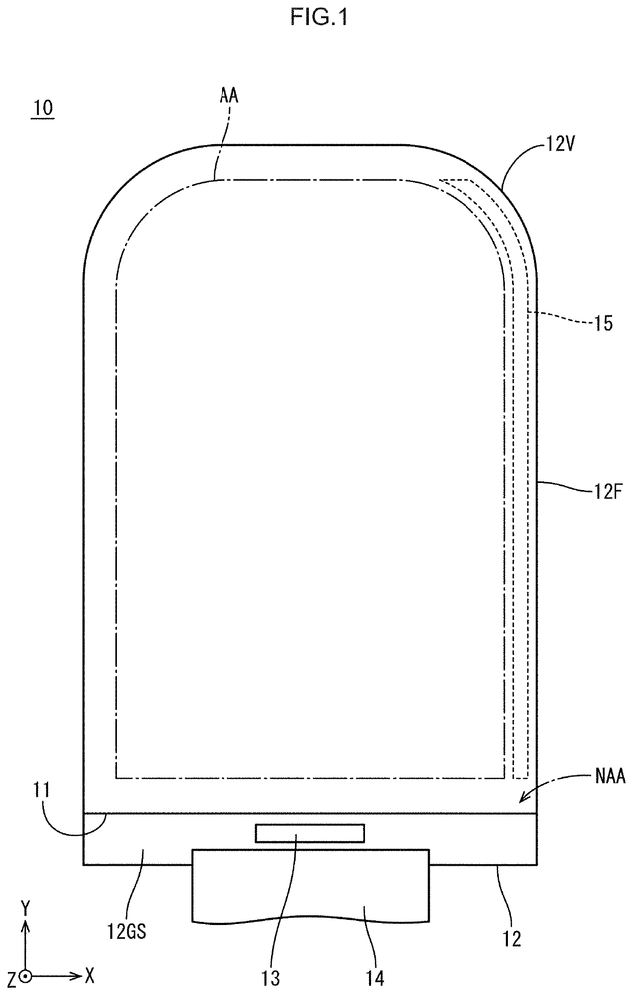
[0030]A first embodiment will be described with reference to FIG. 1 to FIG. 6. In this embodiment, a liquid crystal panel (display device) 10 will be described as an example. Some of these figures illustrate an X axis, a Y axis, and a Z axis, and the figures are drawn in such a manner that the individual axial directions correspond to the directions indicated in the individual figures.

[0031]As illustrated in FIG. 1, the liquid crystal panel 10 according to this embodiment has a planar shape which is vertically-elongated substantially rectangular shape as a whole, and two of the four corner portions thereof are rounded. FIG. 1 is a plan view of the liquid crystal panel 10. In the liquid crystal panel 10, the short-side direction thereof corresponds to an X-axis direction, the long-side direction thereof corresponds to a Y-axis direction, and the thickness direction thereof corresponds to a Z-axis direction. The liquid crystal panel 10 is capable of displaying an image by using illumi...

second embodiment

[0072]A second embodiment will be described with reference to FIG. 7 to FIG. 9. In the second embodiment, the circuit configuration of a unit circuit 120 is different. A duplicate description will be omitted regarding the construction, function, and effect similar to those in the above-described first embodiment.

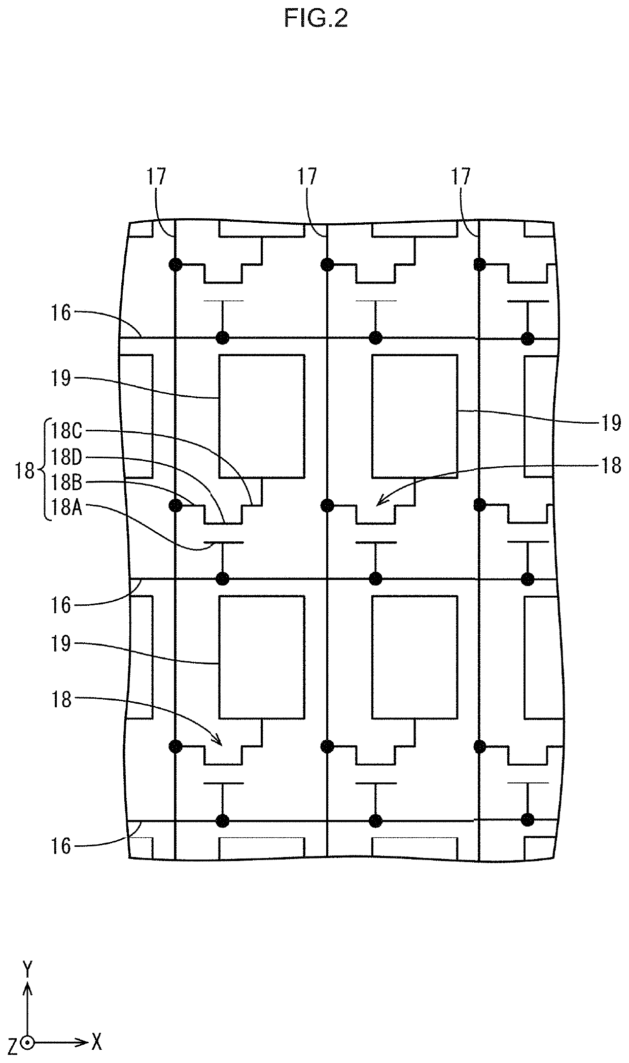
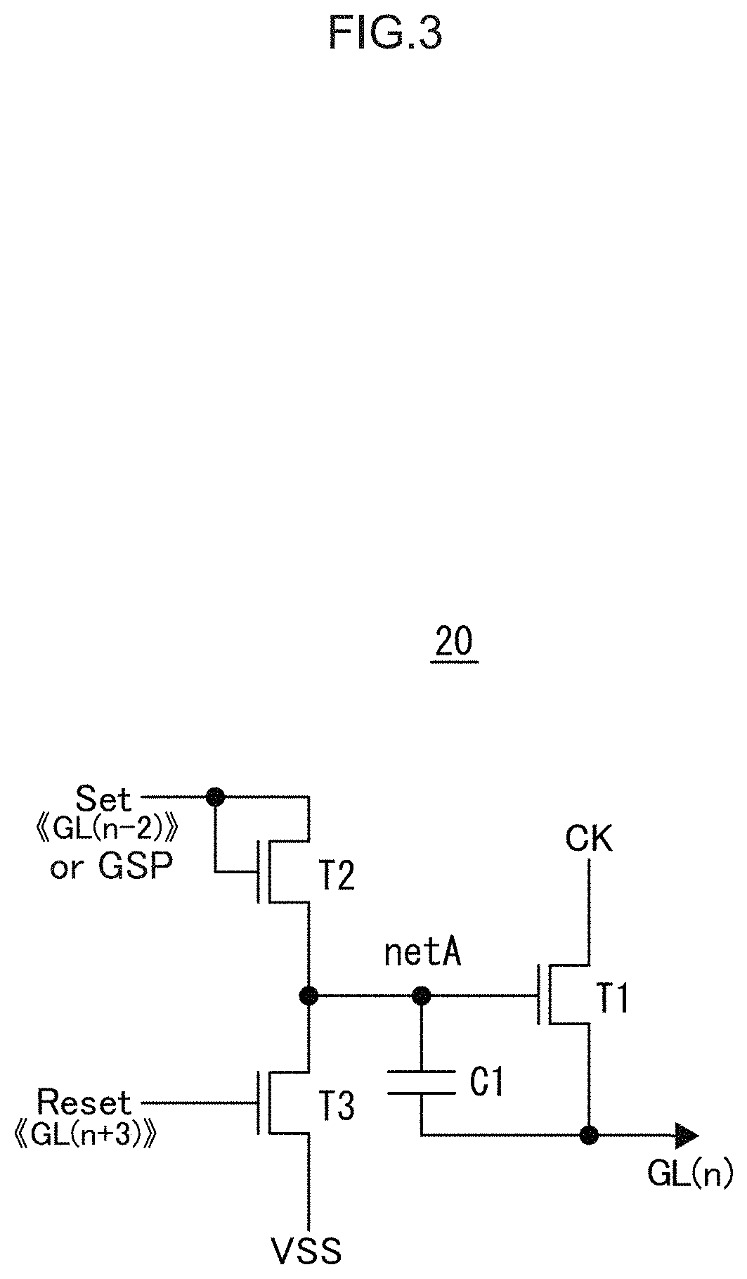
[0073]A specific circuit configuration of the unit circuit 120 according to this embodiment is as illustrated in FIG. 7. FIG. 7 is a circuit diagram illustrating the circuit configuration of the unit circuit 120 constituting a gate circuit portion 115. The unit circuit 120 includes eight gate circuit transistors T11 to T18 and one capacitor C11. Hereinafter, a connection wiring line that connects the gate circuit transistors T11, T12, T15, T16, and T17 and the capacitor C11 to each other will be referred to as an internal node netA. Similarly, a connection wiring line that connects the gate circuit transistors T12, T13, T14, and T17 to each other will be referred to as an in...

third embodiment

[0087]A third embodiment will be described with reference to FIG. 10. The third embodiment is different from the above-described second embodiment in the disposition of a second clock signal wiring line 223 and a power supply voltage signal wiring line 226, and so forth. A duplicate description will be omitted regarding the structure, function, and effect similar to those in the above-described second embodiment.

[0088]The routing of clock signal wiring lines 222 to 225 and the power supply voltage signal wiring line 226 near a variable-external-shape portion 212V according to this embodiment will be described with reference to FIG. 10. FIG. 10 is a plan view schematically illustrating the configuration of the vicinity of the variable-external-shape portion 212V in an array substrate 212. In FIG. 10, the gate start pulse signal wiring line, the set signal wiring lines, and the reset signal wiring lines are not illustrated because the space is limited. In this embodiment, four trunk w...


PUM


Abstract

A circuit substrate includes a substrate portion having a variable-external-shape portion; a circuit portion, having a configuration in which circuit blocks adjacent to each other in a first direction; a plurality of trunk wiring lines bent along the circuit blocks displaced with respect to each other in a second direction; and a plurality of branch wiring lines, wherein the plurality of trunk wiring lines include a first trunk wiring line and a second trunk wiring line, and among the plurality of branch wiring lines, a plurality of branch wiring lines connected to a plurality of unit circuits constituting a center-side circuit block include at least a first branch wiring line connected to the first trunk wiring line and a second branch wiring line connected to the second trunk wiring line and disposed farther than the first branch wiring line from a end-side circuit block in the first direction.

Description

CROSS-REFERENCE TO RELATED APPLICATION[0001]The present application claims priority from Provisional Application No. 62 / 963,587, the content to which is hereby incorporated by reference into this application.BACKGROUND1. Field[0002]The techniques disclosed in this description relate to a circuit substrate and a display device.2. Description of the Related Art[0003]Hitherto, as an example of an element substrate of an electrooptical device, the element substrate described in Japanese Unexamined Patent Application Publication No. 2009-122636 has been known. In the element substrate of the electrooptical device described in Japanese Unexamined Patent Application Publication No. 2009-122636, a pixel region has an odd-shaped outer peripheral portion formed of a curved portion at a portion opposed to a scanning line driving circuit. In the scanning line driving circuit, in accordance with such a shape, circuit blocks each having a unit circuit block including one or a plurality of unit ci...

Claims


Application Information

Patent Timeline
IPC IPC(8): H01L27/12G02F1/1362
CPCH01L27/124G02F1/136286
Inventor ASAIHORIUCHI, SATOSHIKAWAMORITA, SEIYAMATSUBARA, SHINJIGYOUTEN, SEIJIROU
Owner SHARP KK
Why Eureka
Try Eureka