Light emitting device, backlight, and display panel

Active Publication Date: 2022-05-26
LEXTAR ELECTRONICS CORP
View PDF9 Cites 0 Cited by
  • Summary
  • Abstract
  • Description
  • Claims
  • Application Information

AI Technical Summary

Benefits of technology

The patent aims to provide a light emitting device, backlight, and display panel that can address the problems of overvoltage, excessive power consumption, and malfunctions in conventional display devices.

Problems solved by technology

However, various existing COB packaging technology still have many problems such as high production costs, serious light loss, and poor product stabilities.

Method used


Image

  • Light emitting device, backlight, and display panel
  • Light emitting device, backlight, and display panel
  • Light emitting device, backlight, and display panel

Examples


Embodiment Construction

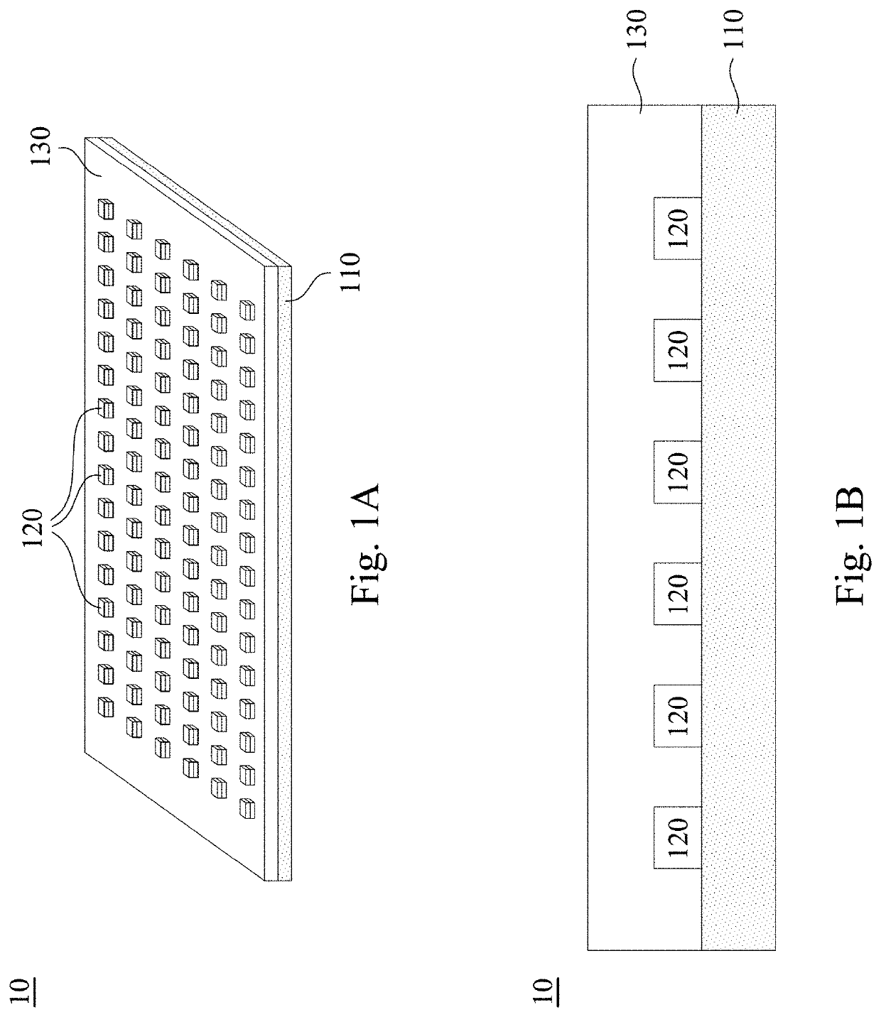
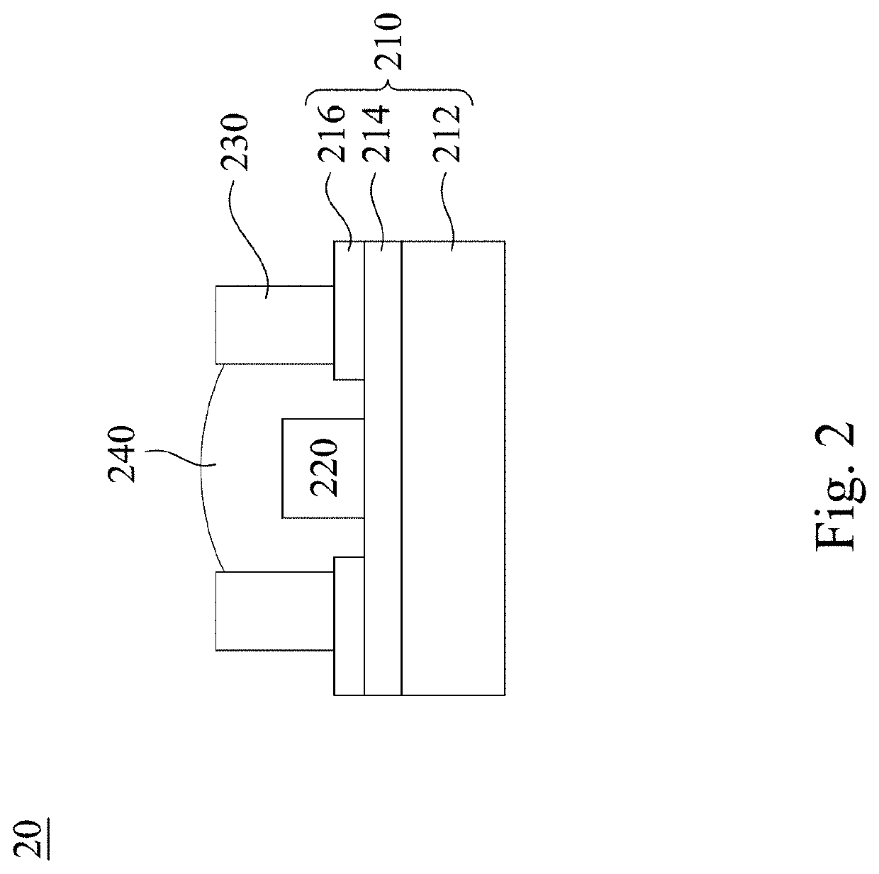
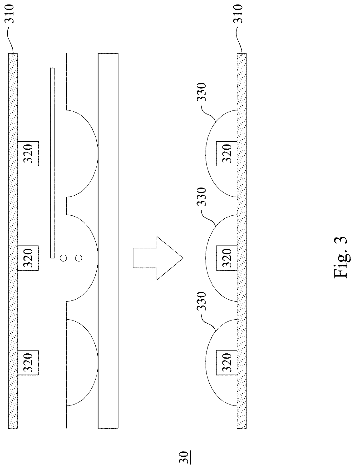
[0037]The following disclosure provides many different embodiments, or examples, for implementing different features of the provided subject matter. Specific examples of components and arrangements are described below to simplify the present disclosure. These are, of course, merely examples and are not intended to be limiting. The embodiments disclosed below may be combined or substituted with each other under beneficial circumstances, and other embodiments may also be added to an embodiment without further description.

[0038]It will be understood that, although the terms “first,”“second,”“third” etc. may be used herein to describe various elements, components, regions, layers and / or sections, these elements, components, regions, layers and / or sections should not be limited by these terms. These terms are only used to distinguish one element, component, region, layer or section from another element, component, region, layer or section. Thus, a first element, component, region, layer ...


PUM


Abstract

The present disclosure provides a light emitting device including a substrate, a conductive layer, first and second reflective layers, a light emitting element, and an encapsulation layer. The conductive layer is disposed on the substrate. The first reflective layer covers the conductive layer and has an opening exposing a portion of the conductive layer. The light emitting element is disposed in the opening and electrically connects to the conductive layer. The second reflective layer is disposed on the first reflective layer and surrounds the light emitting element, and the second reflective layer has an outer diameter. The encapsulation layer covers the light emitting element. There is a height between a highest point of the encapsulation layer and an upper surface of the first reflective layer, and the height is 0.1 to 0.5 times the outer diameter. The present disclosure also provides a backlight and a display panel.

Description

CROSS-REFERENCE TO RELATED APPLICATION[0001]This application claims priority to China Application Serial Number 202011306944.3, filed Nov. 20, 2020, which is herein incorporated by reference.BACKGROUNDField of Invention[0002]The present disclosure relates to a light emitting device, a backlight, and a display panel.Description of Related Art[0003]With the advancement of light emitting diode technologies and increasing market demand, novel display technologies represented by mini-light emitting diodes / micro-light emitting diodes (Mini-LEDs / Micro-LEDs) have emerged.[0004]The Mini-LED packaging mainly includes chip on board (COB) technology and integrated mounted device (IMD) packaging technology. The COB technology is to directly mount the LED chip on the module substrate, and then mold each large unit as a whole. However, various existing COB packaging technology still have many problems such as high production costs, serious light loss, and poor product stabilities.SUMMARY[0005]In v...

Claims


Application Information

Patent Timeline
IPC IPC(8): G02F1/13357H01L33/00H01L33/54H01L33/60G02F1/1335
CPCG02F1/133603H01L33/005H01L33/54H01L33/60G02F2202/36G02F1/133607G02F1/133611H01L2933/005H01L2933/0058G02F1/133614H01L33/46H01L27/156G02F1/133606H01L33/62H01L25/0753H01L33/56H01L33/507H01L2933/0091H01L33/504
Inventor TIEN, YUN-YIWU, YU-CHANGCHANG, YU-LI
Owner LEXTAR ELECTRONICS CORP
Why Eureka
Try Eureka