Pixel circuit and driving method thereof

a technology of pixel circuit and driving method, which is applied in the direction of instruments, static indicating devices, etc., can solve the problems of deterioration of contrast, inability to acquire original white display brightness, and inability to acquire brightness

Active Publication Date: 2018-05-03
TIANMA MICRO ELECTRONICS CO LTD
View PDF1 Cites 9 Cited by
  • Summary
  • Abstract
  • Description
  • Claims
  • Application Information

AI Technical Summary

Benefits of technology

[0092]As an exemplary advantage according to the invention, the present invention makes it possible to prevent image retention through applying a constant voltage to the driving transistor before having the voltage containing the threshold voltage and the data voltage held to the capacitor part.

Problems solved by technology

However, the existing pixel circuit with a threshold voltage detecting function has following issues.
Therefore, the brightness of the original white display cannot be acquired.
(2) Due to leaked light emission in a non-emission period, the contrast deterioration occurs.
Therefore, leaked light emission is generated, and the electric current flown to the driving transistor 14 cannot be brought up to the prescribed bias current.
Therefore, leaked light emission is generated, and the prescribed bias current cannot be flown to the driving transistor 96.

Method used


Image

  • Pixel circuit and driving method thereof
  • Pixel circuit and driving method thereof
  • Pixel circuit and driving method thereof

Examples


first exemplary embodiment

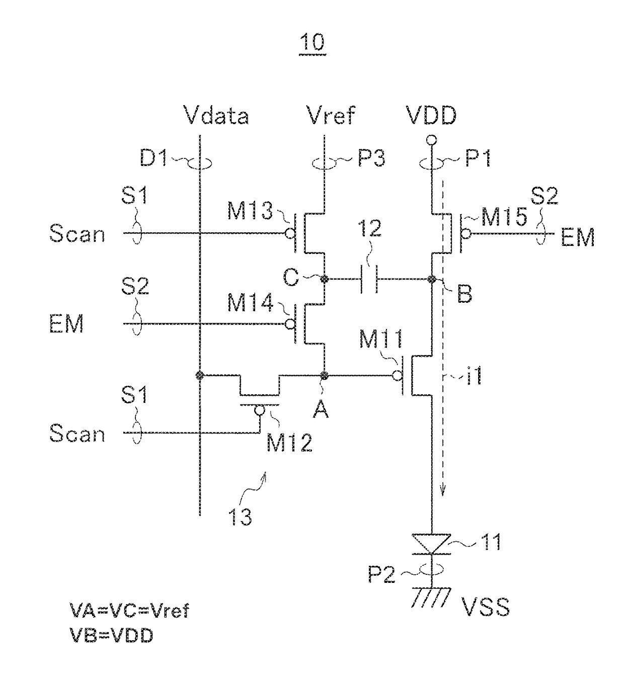
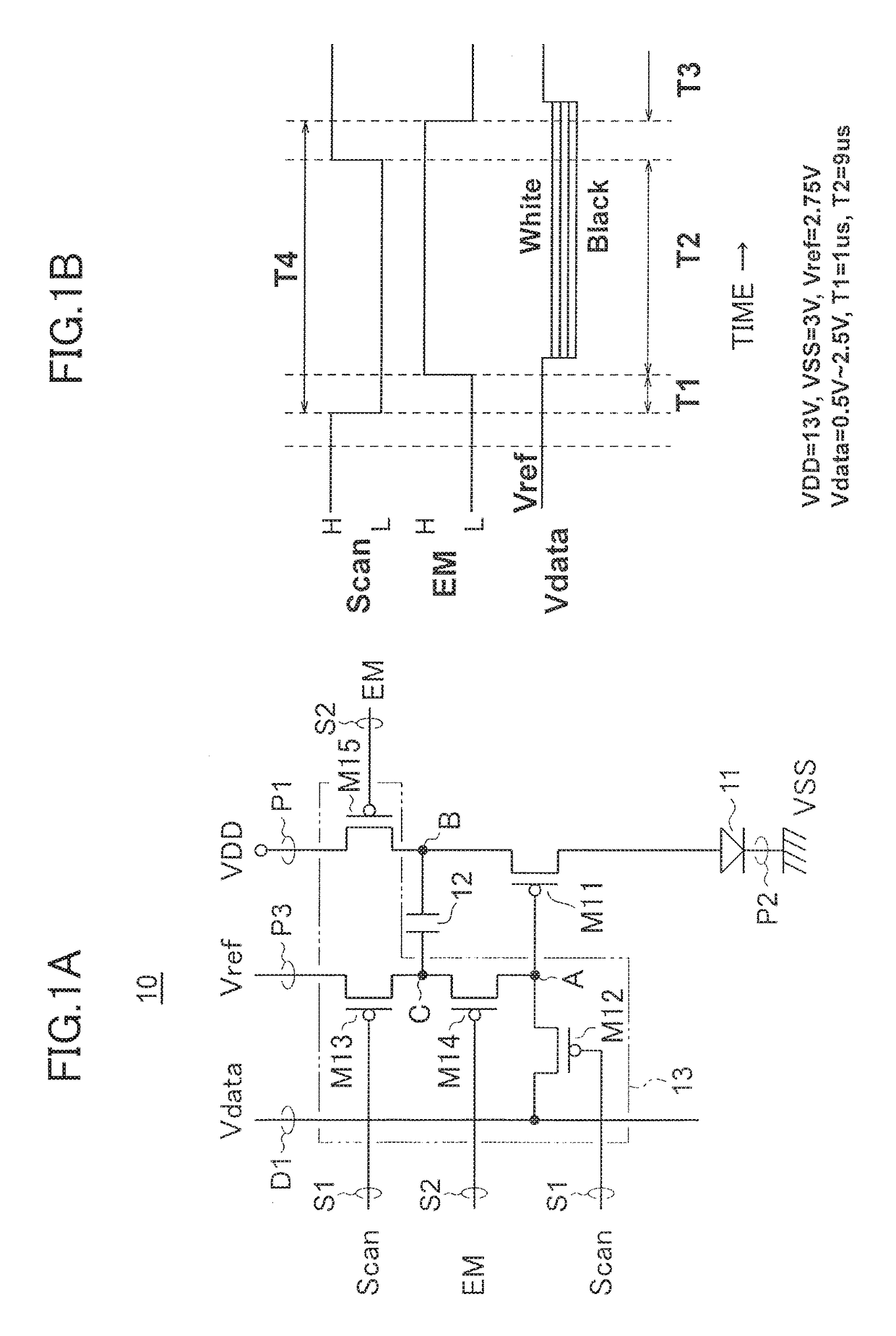
[0048]FIG. 1A is a circuit diagram showing the structure of a pixel circuit according to a first exemplary embodiment, and FIG. 1B is a timing chart showing operations of the pixel circuit of the first exemplary embodiment. Explanations will be provided hereinafter by referring to those drawings.

[0049]A pixel circuit 10 of the first exemplary embodiment includes: a light emitting element 11; a driving transistor (M11) which supplies an electric current to the light emitting element 11 according to an applied voltage; a capacitor part (12) which holds a voltage containing a threshold voltage Vth and a data voltage Vdata of the driving transistor (M11); and a switch part 13 which has the voltage containing the threshold voltage Vth and the data voltage Vdata held to the capacitor part (12) and applies these voltage to the driving transistor (M11). Further, the switch part 13 has a function which applies a constant voltage for preventing initialization of hysteresis characteristics to ...

second exemplary embodiment

[0093]FIG. 7A is a circuit diagram showing the structure of a pixel circuit according to a second exemplary embodiment, and FIG. 7B is a timing chart showing operations of the pixel circuit of the second exemplary embodiment. Explanations will be provided hereinafter by referring to those drawings.

[0094]A pixel circuit 20 of the second exemplary embodiment is different from that of the first exemplary embodiment in respect that a switch part 23 includes a current detour transistor (M16). The current detour transistor (M16) makes the electric current supplied from the driving transistor (M11) detour without flowing through the light emitting element 11.

[0095]Further, the switch part 13 turns on the driving transistor (M11) and the current detour transistor (M16) before having the voltage containing the threshold voltage Vth and the data voltage Vdata of the driving transistor (M11) held to the capacitor part (12).

[0096]In more detail, the switch part 23 turns on the current detour tr...

third exemplary embodiment

[0117]FIG. 11A is a circuit diagram showing the structure of a pixel circuit according to a third exemplary embodiment, and FIG. 11B is a timing chart showing operations of the pixel circuit of the third exemplary embodiment. Explanations will be provided hereinafter by referring to those drawings.

[0118]The third embodiment employs the structure in which: all the transistors of the second exemplary embodiment are replaced with the n-channel types while keeping the second terminal (cathode terminal) of the light emitting element 11 on the substrate side (VSS side); and the layout of the capacitor part (12) connected between the gate and the source as well as the accompanying transistors is changed accordingly. Therefore, the threshold voltage detecting module of the third exemplary embodiment is also a source follower type that is the same as the case of the second exemplary embodiment.

[0119]That is, the outline of a pixel circuit 30 according to the third exemplary embodiment can be...


PUM


Abstract

To prevent image retention, the pixel circuit includes: a light emitting element; a driving transistor which supplies an electric current according to an applied voltage to the light emitting element; a capacitor part which holds the voltage containing a threshold voltage and a data voltage of the driving transistor; and a switch part which has the voltage containing the threshold voltage and the data voltage held to the capacitor part and applies the voltage to the driving transistor. Further, the switch part has a function which applies a constant voltage to the driving transistor before having the voltage containing the threshold voltage and the data voltage held to the capacitor part.

Description

CROSS-REFERENCE TO RELATED APPLICATION[0001]This application is a Divisional of U.S. application Ser. No. 14 / 752,218 filed on Jun. 26, 2015, which claims priority from Japanese Patent Application No. 2014-133382, filed on Jun. 27, 2014 and Japanese Patent Application No. 2015-031373, filed on Feb. 20, 2015, the disclosures of which are incorporated herein by reference in their entireties.BACKGROUND OF THE INVENTION1. Field of the Invention[0002]The present invention relates to a pixel circuit and a driving method used in an Active Matrix Organic Light Emitting Display (referred to as “AMOLED”, hereinafter) and the like. An organic light emitting diode is also referred to as an organic EL element (referred hereinafter as “OLED”).2. Description of the Related Art[0003]There is no standard pixel circuit of AMOLED, so that each of the companies manufacturing AMOLED uses their original pixel circuits. A typical pixel circuit is provided with OLED, a drive transistor for driving the OLED,...

Claims


Application Information

Patent Timeline
Patent Type & Authority Applications(United States)
IPC IPC(8): G09G3/325G09G3/3233
CPCG09G2320/045G09G2320/0257G09G2320/0238G09G2300/08G09G2300/0842G09G3/325G09G3/3233G09G2300/0895
Inventor NONAKA, YOSHIHIROMATSUEDA, YOJIROTAKATORI, KENICHI
Owner TIANMA MICRO ELECTRONICS CO LTD
Why Eureka
Try Eureka