Resin composition for light blocking member and display panel comprising the same
a technology of light blocking member and composition, which is applied in the direction of synthetic resin layered products, instruments, organic chemistry, etc., can solve the problems of shortcoming of alignment and afterimage incursion, and achieve the effects of reducing parasitic capacitance, preventing afterimage incursion, and high optical density
- Summary
- Abstract
- Description
- Claims
- Application Information
AI Technical Summary
Benefits of technology
Problems solved by technology
Method used
Image
Examples
first exemplary embodiment
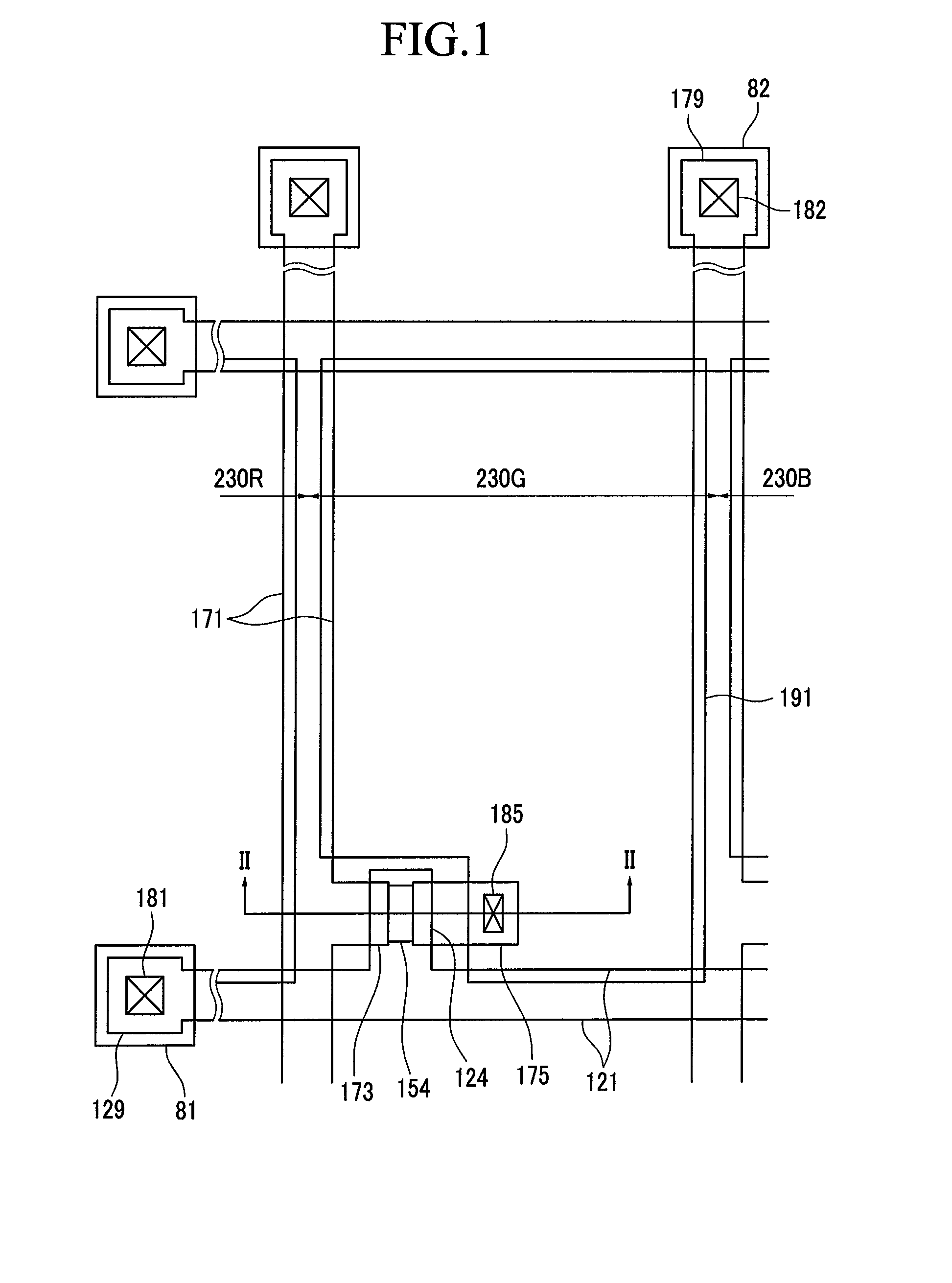
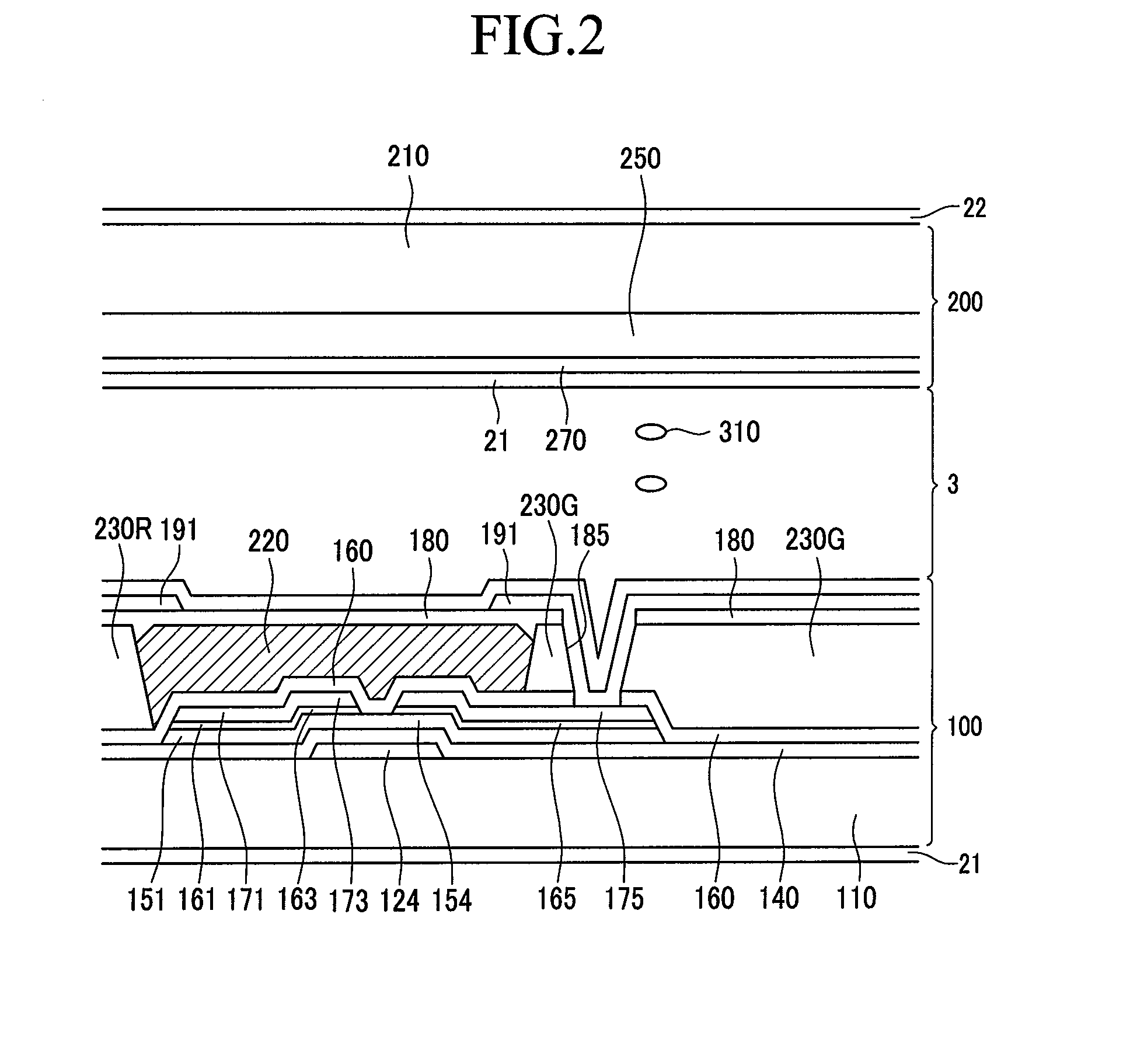
[0045]Hereinafter, a liquid crystal display according to an exemplary embodiment of the present invention will be described with reference to FIG. 1 and FIG. 2.
[0046]FIG. 1 is a layout view of a liquid crystal display according to an exemplary embodiment of the present invention, and FIG. 2 is a cross-sectional view of a liquid crystal display shown in FIG. 1 taken along the line II-II.
[0047]Referring to FIG. 1 and FIG. 2, the liquid crystal display according to an exemplary embodiment of the present invention includes a thin film transistor array panel 100, a common electrode panel 200 facing the thin film transistor array panel 100, and a liquid crystal layer 3 interposed between the thin film transistor array panel 100 and the common electrode panel 200.
[0048]Hereinafter, the thin film transistor array panel 100 will be described.
[0049]A plurality of gate lines 121 are formed on an insulating substrate 110 to transmit a gate signal. Each of the gate lines 121 includes an end port...
second exemplary embodiment
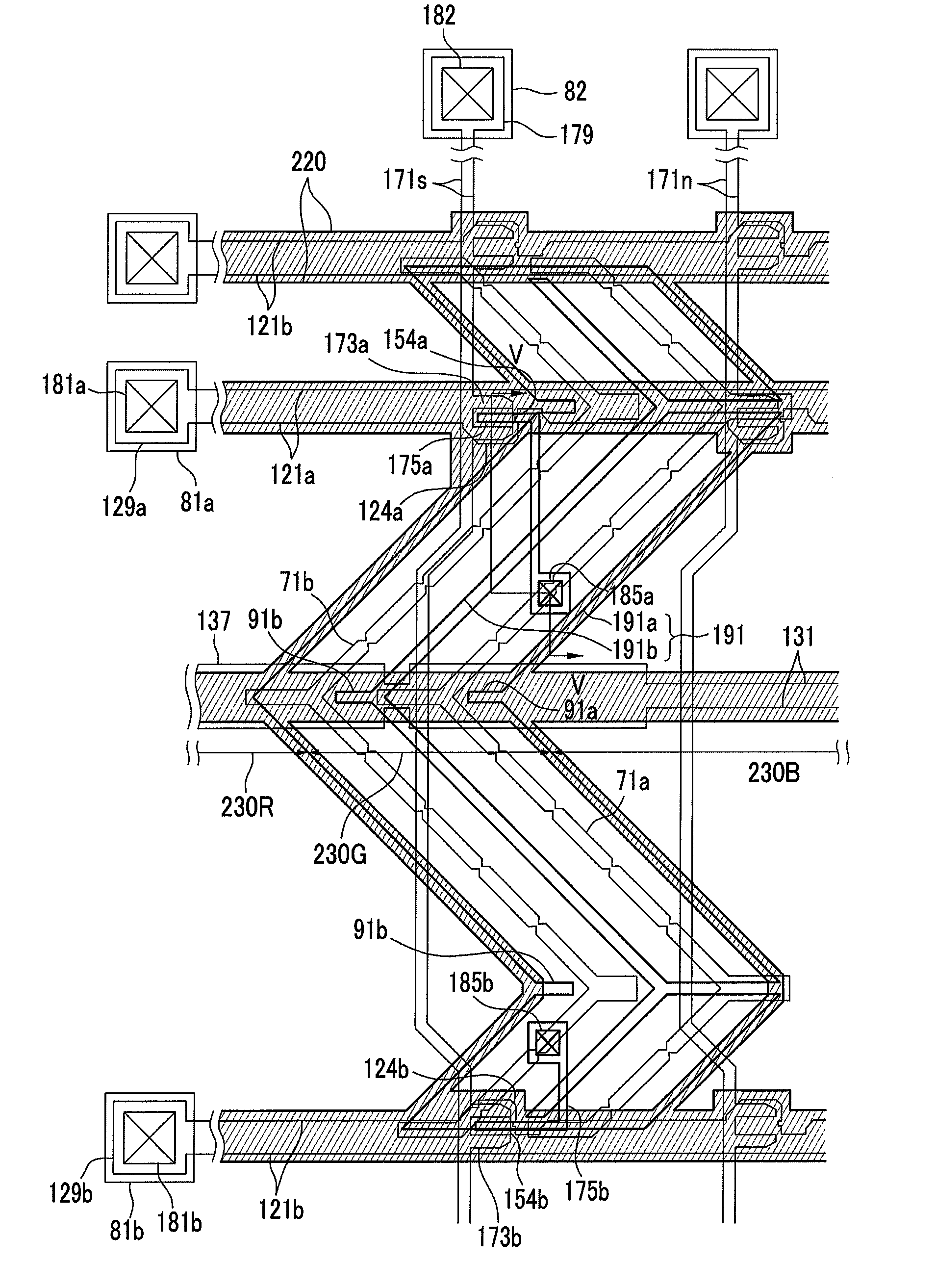
[0090]Hereinafter, a liquid crystal display according to another exemplary embodiment of the present invention will be described with reference to FIG. 3 to FIG. 5. Descriptions of like elements are omitted.
[0091]FIG. 3 is an equivalent circuit diagram for one pixel of a liquid crystal display according to another exemplary embodiment of the present invention. FIG. 4 is a layout view of a liquid crystal display of FIG. 3, FIG. 5 is a cross-sectional view of a liquid crystal display shown in FIG. 4 taken along the line V-V, and FIG. 6 is a layout view of a pixel electrode and a common electrode in a liquid crystal display shown in FIG. 4 and FIG. 5.
[0092]Referring to FIG. 3, each pixel PX includes a pair of subpixels PXa and PXb. Each of the subpixels PXa and PXb includes a switching element Qa or Qb connected to a corresponding gate line 121a or 121b and a data line 171s, a liquid crystal capacitor Clca or Clcb connected to the switching element Qa or Qb, and a storage capacitor Cst...
PUM
| Property | Measurement | Unit |
|---|---|---|
| optical density | aaaaa | aaaaa |
| optical density | aaaaa | aaaaa |
| optical density | aaaaa | aaaaa |
Abstract
Description
Claims
Application Information


