
Eureka
For R&D, Eureka makes reading and utilizing patents & technical documents easy.
Eureka AIR
Designed for self-driven R&D workflows. Generate viable solutions, solve complex R&D challenges, empower your innovation with AI.

Eureka Materials
Designed for material experts only. Revolutionize your material R&D, from search, analyze, to developing new materials.

TechResearch
Generate reliable direction feasibility study reports for your R&D in just a few steps.

TechSeek
Discover and master advanced knowledge NOW. Basics, ideas, possibilities, all at once.

TechMind
As an expert in R&D Theories, TechMind can generates customized viable solutions instantly.

TechRisk
Analyze your overall solution with one click, know your potential R&D risks in advance.

TechMonitor
Get weekly tech updates, stay abreast of the latest tech innovations and key insights.
Thin-film piezoelectric material element having a solder regulating part formed on a pad surface being a surface of an electrode pad
- Summary
- Abstract
- Description
- Claims
- Application Information
AI Technical Summary
Benefits of technology
Problems solved by technology
Method used
Image

Examples
modified example
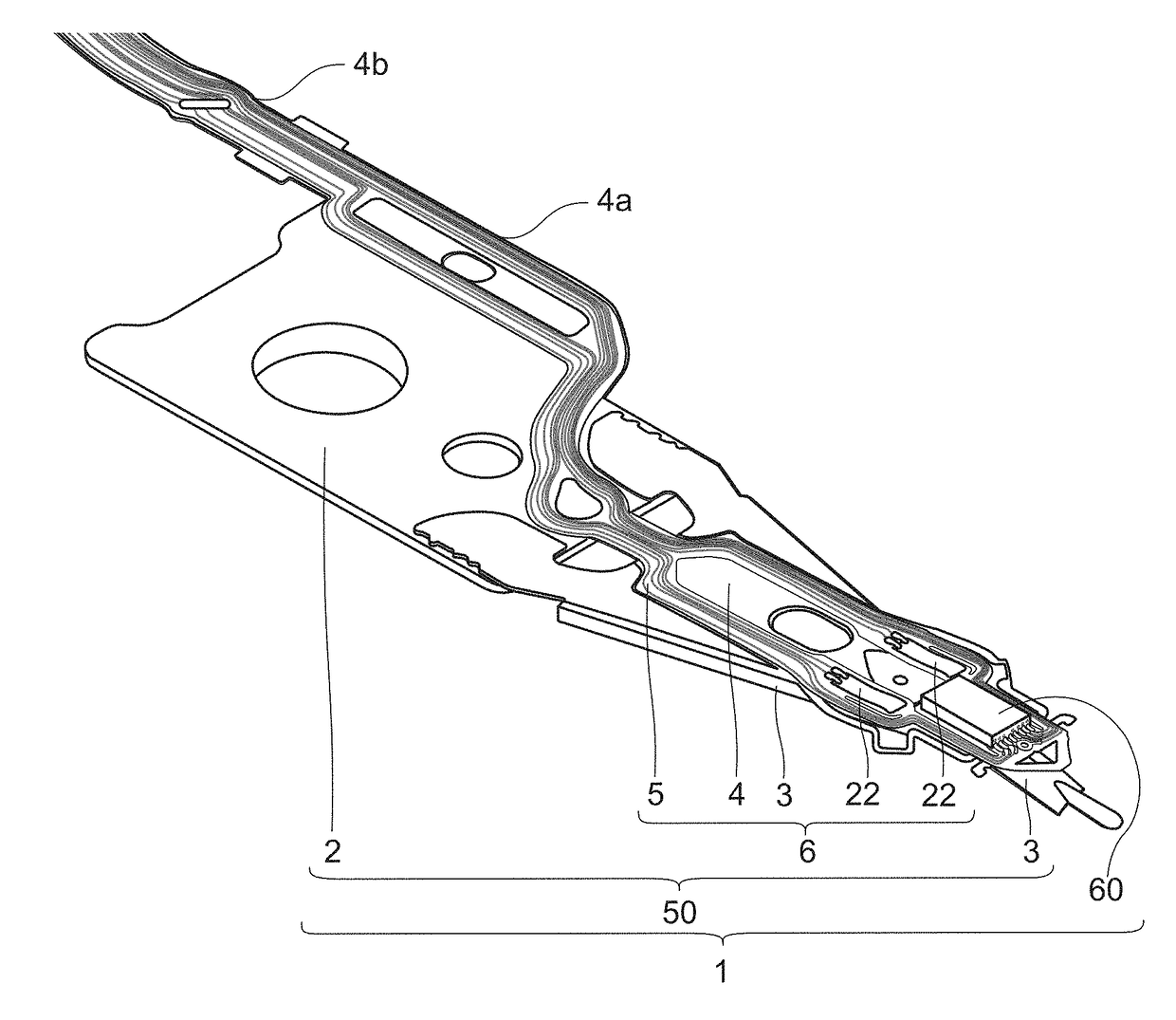
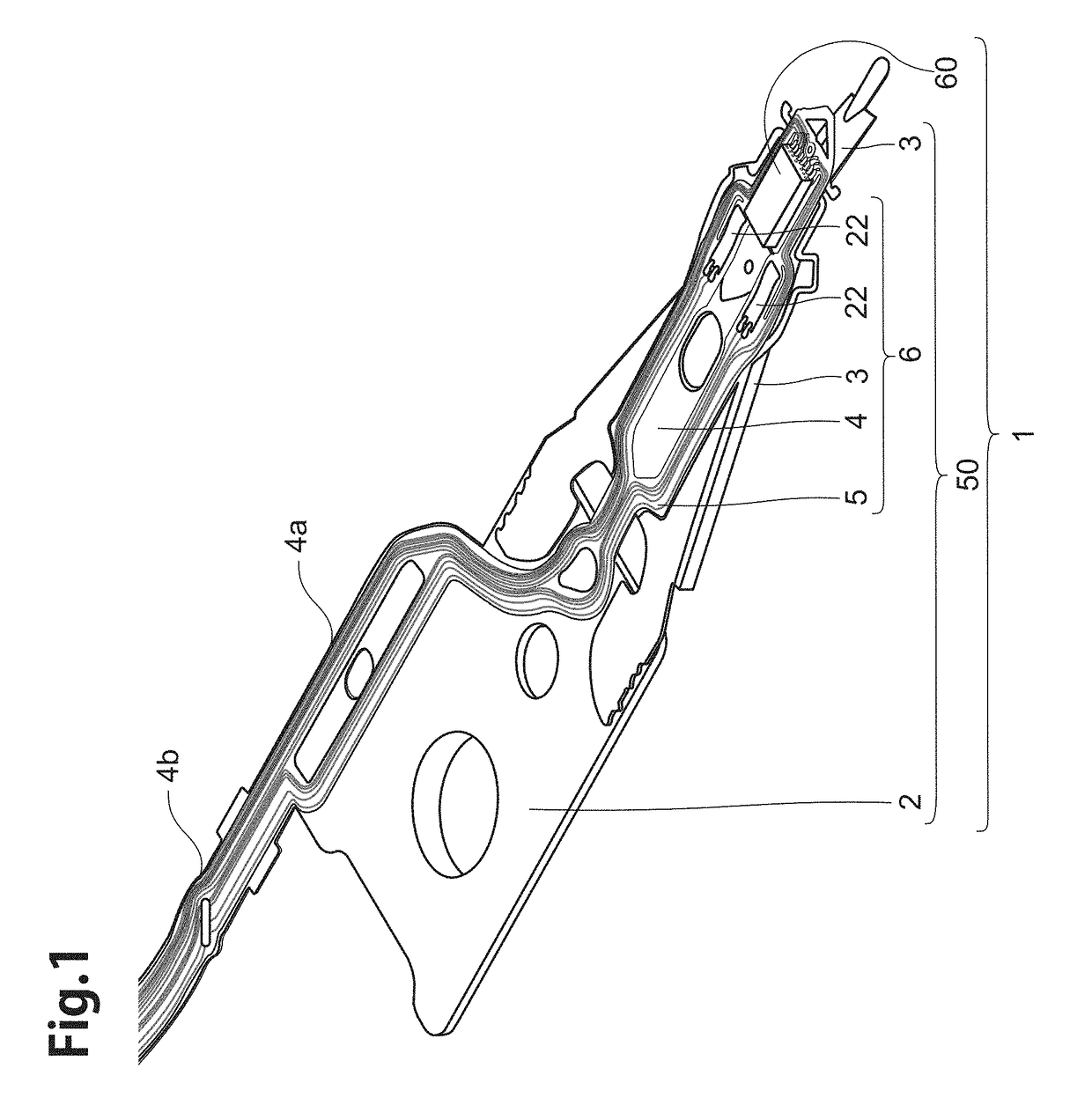
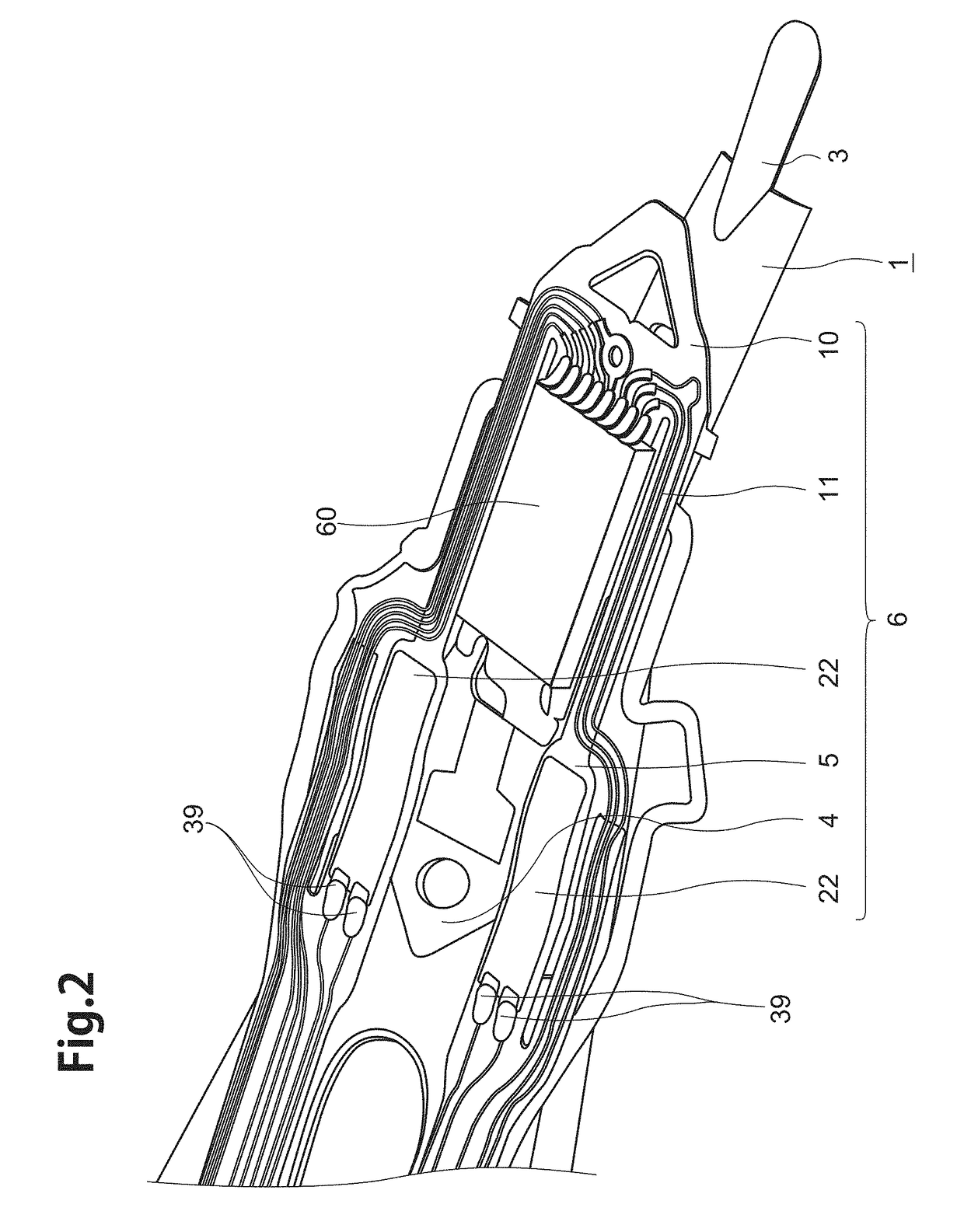
[0093]It is possible that the thin-film piezoelectric material element 22 has the solder regulating parts 135 instead of the above-described solder regulating parts 30. The solder regulating parts 135 are different from the solder regulating parts 30 in that the solder regulating parts 135 have the crossing edge parts 134 instead of the crossing edge parts 33, as illustrated in FIG. 11.
[0094]The crossing edge parts 134 do not have the flat parts 32 like the crossing edge parts 33, and the crossing edge parts 134 are composed of entirely curved surfaces which connect the outer edge parts 34a with the outer edge parts 34b. The crossing edge parts 134 are also warped in a bow shape with a receding direction from the shortest lines 36, and the crossing edge parts 134 are formed in a bow like curve-shape, similar with the crossing edge parts 33.
[0095]Because unevenness of surface density, about the solder applied on the electrode pads 29, does not appear, when the thin-film piezoelectric...
PUM
 Abstract
Description
Claims
Application Information
 - R&D Engineer
- R&D Manager
- IP Professional
- Industry Leading Data Capabilities
- Powerful AI technology
- Patent DNA Extraction
Browse by: Latest US Patents, China's latest patents, Technical Efficacy Thesaurus, Application Domain, Technology Topic, Popular Technical Reports.
© 2024 PatSnap. All rights reserved.Legal|Privacy policy|Modern Slavery Act Transparency Statement|Sitemap|About US| Contact US: help@patsnap.com