Organic light-emitting display device

a display device and light-emitting technology, applied in the direction of organic semiconductor devices, solid-state devices, semiconductor devices, etc., can solve the problems of inability to fill the undercut of inorganic film, gap formation, and organic layer may be stained

Active Publication Date: 2018-05-31
LG DISPLAY CO LTD
View PDF10 Cites 31 Cited by
  • Summary
  • Abstract
  • Description
  • Claims
  • Application Information

AI Technical Summary

Benefits of technology

[0010]One of the object a of the present disclosure is to provide an organic light-emitting display device configured such that the undercut shape of an auxiliary electrode is improved and such that a region where the auxiliary electrode and a second electrode contact is filled with an inorganic film, whereby a gap is prevented from being formed and the reliability of the organic light-emitting display device is improved.
[0013]In one embodiment, the reverse taper-shaped end of the passivation layer overlies the exposed side surface of the auxiliary electrode. In this embodiment, the reverse taper-shaped end provides for easy exposure of the side surface of the auxiliary electrode. In one embodiment, the side surface of the auxiliary electrode has a positive taper, but this is not required in all embodiments.

Problems solved by technology

In an organic light-emitting display device having such an undercut-shaped passivation layer, when an inorganic film is formed after an organic layer including an emissive layer has been formed, the inorganic film cannot fill the undercut-shaped lower part of the passivation layer, with the result that a gap is formed.
The impurities damage the organic layer, with the result that the organic layer may be stained.
In addition, the mechanical properties of the organic light-emitting display device may be deteriorated, whereby the reliability of the organic light-emitting display device may be reduced.

Method used


Image

  • Organic light-emitting display device
  • Organic light-emitting display device
  • Organic light-emitting display device

Examples


Embodiment Construction

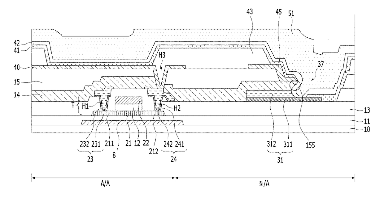
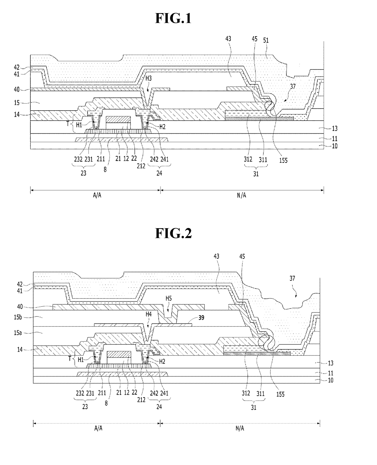
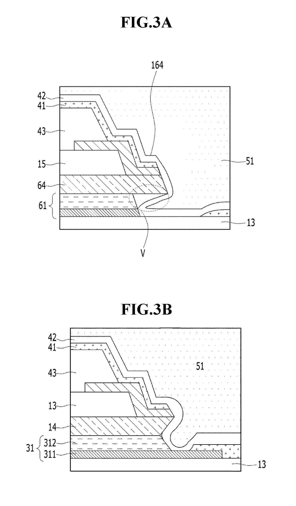
[0021]Reference will now be made in detail to the preferred embodiments of the present disclosure, examples of which are illustrated in the accompanying drawings. Wherever possible, the same reference numbers will be used throughout the drawings to refer to the same or like parts. In the following description of the present disclosure, a detailed description of known functions and configurations incorporated herein will be omitted when it may obscure the subject matter of the present disclosure. In addition, the terms used in the following description are selected in consideration of ease of preparation of the specification, and may be different from the names of parts constituting an actual product.

[0022]It will be understood that when an element is referred to as being “on,”“above,”“under” or “beside” another element, one or more intervening elements may be present therebetween, as long as the term “immediately” or “directly” is not used.

[0023]It may be understood that, although t...


PUM


Abstract

Disclosed is an organic light-emitting display device configured such that the undercut shape of an auxiliary electrode is improved and such that a region where the auxiliary electrode and a second electrode contact is filled with an inorganic film, whereby a gap is prevented from being formed and the reliability of the organic light-emitting display device is improved. The organic light-emitting display device includes a first electrode located on a substrate defined by an active area and a non-active area, an organic layer including an emissive layer located on the first electrode, a second electrode located on the organic layer, an auxiliary electrode located in the non-active area, and a passivation layer located on the auxiliary electrode, the passivation layer having a reverse taper-shaped end so as to be exposed to the side surface of the auxiliary electrode. The second electrode extends to the non-active area so as to be electrically connected to the exposed auxiliary electrode. In addition, the auxiliary electrode has a taper-shaped end under the passivation layer.

Description

[0001]This application claims the benefit of Korean Patent Application No. 10-2016-0162362, filed on Nov. 30, 2016, which is hereby incorporated by reference as if fully set forth herein.BACKGROUNDTechnical Field[0002]The present disclosure relates to an organic light-emitting display device, and more particularly to an organic light-emitting display device that is capable of achieving contact with an auxiliary electrode using an undercut structure, whereby the reliability of the organic light-emitting display device is improved.Description of the Related Art[0003]Image display devices, which are a core technology in the information and communication age and serve to display various kinds of information on a screen, have been developed such that the image display devices are thinner, lighter, and portable and exhibit high performance. In addition, organic light-emitting display devices, which control the amount of light that is emitted from an organic light-emitting layer to display...

Claims


Application Information

Patent Timeline
Patent Type & Authority Applications(United States)
IPC IPC(8): H01L51/52H01L51/50H01L27/32H01L51/56
CPCH01L51/5228H01L51/5012H01L51/5206H01L51/5253H01L27/3223H01L27/3258H01L27/3262H01L27/3272H01L51/56H01L2251/308H01L2251/301H01L2227/323H10K59/12H10K50/824H10K59/1201H10K50/844H10K59/124H10K59/1315H10K59/88H10K59/123H10K59/1213H10K59/131H10K50/11H10K50/81H10K59/126H10K71/00H10K2102/00H10K2102/103
Inventor LEE, JAE-SUNGIM, JONG-HYEOKKIM, DO-HYUNG
Owner LG DISPLAY CO LTD
Why Eureka
Try Eureka