Multi-aperture imaging device having a beam-deflecting device comprising reflecting facets

Active Publication Date: 2018-06-21
FRAUNHOFER GESELLSCHAFT ZUR FOERDERUNG DER ANGEWANDTEN FORSCHUNG EV
View PDF8 Cites 9 Cited by
  • Summary
  • Abstract
  • Description
  • Claims
  • Application Information

AI Technical Summary

Benefits of technology

[0006]The core idea of the present invention is the finding that that a beam-deflecting device can be produced cost-effectively and without any losses of optical quality of the multi-aperture imaging device when a carrier substrate is provided for the same, wherein the carrier substrate is common to the plurality of optical channels and is installed with a setting angle, i.e. oblique with respect to the image sensor in the multi-aperture imaging device such that a deflection angle of deflecting the optical path of each optical channel is based, on the one hand, on the setting angle and, on the other hand, on an individual inclination angle w

Problems solved by technology

Multi-aperture imaging devices are in particular used in applications where a single-aperture imaging device would have disadvantages with regard to the installation size.
In particular in the low-cost sector it is difficult to produce the facets with, on the one hand, sufficient optical accuracy for preventing image errors and, on the other hand, in a cost-effective manner.
Forming a prism of polymer, for example, which comprises a facet-

Method used


Image

  • Multi-aperture imaging device having a beam-deflecting device comprising reflecting facets
  • Multi-aperture imaging device having a beam-deflecting device comprising reflecting facets
  • Multi-aperture imaging device having a beam-deflecting device comprising reflecting facets

Examples


Example

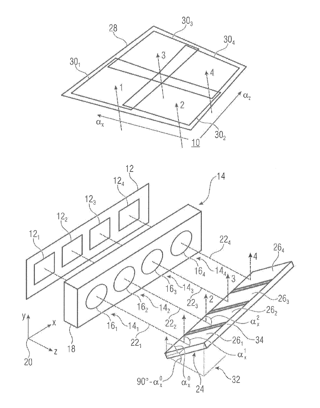
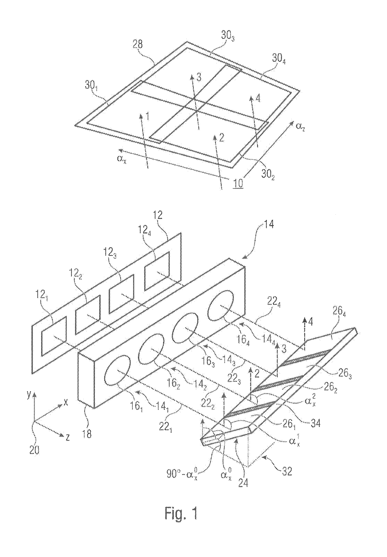
[0027]FIG. 1 shows an embodiment of a multi-aperture imaging device. The multi-aperture imaging device 10 of FIG. 1 includes an image sensor 12 and a plurality 14 of optical channels, each of which being defined by respective optics 161, 162, 163 and 164. Each optical channel 141, 142, 143, 144 projects, by means of the allocated optics 161-164, a channel-individual section of a total field of view of the multi-aperture imaging device 10 on a respective image sensor area 121, 122, 123 or 124. The image sensor 12 can, for example, be a chip comprising pixel arrays in the image sensor areas 121-124. Alternatively, the image sensor 12 could comprise one pixel array chip per image sensor area 121-124. Again, it would be possible that the image sensor 12 comprises a pixel array extending continuously across the image sensor areas 121-124, i.e. a pixel array having a rectangular or varying extension in which the image sensor areas 121-124 lie, wherein in that case, for example, merely the...


PUM


Abstract

The fact that a beam-deflecting device can be produced cost-effectively and without any losses of optical quality of the multi-aperture imaging device is used when a carrier substrate is provided for the same, wherein the carrier substrate is common to the plurality of optical channels and is installed with a setting angle, i.e. oblique with respect to the image sensor in the multi-aperture imaging device such that a deflection angle of deflecting the optical path of each optical channel is based, on the one hand, on the setting angle and, on the other hand, on an individual inclination angle with respect to the carrier substrate of a reflecting facet of a surface of the beam-deflecting device facing the image sensor, the reflecting facet being allocated to the optical channel.

Description

CROSS-REFERENCE TO RELATED APPLICATIONS[0001]This application is a continuation of copending International Application No. PCT / EP2016 / 069630, filed Aug. 18, 2016, which is incorporated herein by reference in its entirety, and additionally claims priority from German Application No. 10 2015 215 836.5, filed Aug. 19, 2015, which is also incorporated herein by reference in its entirety.[0002]The present invention relates to a multi-aperture imaging device having a beam-deflecting device comprising reflecting facets.BACKGROUND OF THE INVENTION[0003]Multi-aperture imaging devices are in particular used in applications where a single-aperture imaging device would have disadvantages with regard to the installation size. For example, different portions of a field of view of a total field of view are projected on different areas of an image sensor. This takes place via several optical channels, wherein each channel is defined by a respective optic which performs projecting on the respective ...

Claims


Application Information

Patent Timeline
IPC IPC(8): H04N5/225
CPCH04N5/2259H04N5/2258H04N5/2254H04N23/58H04N23/45H04N23/55G03B2205/0007G02B27/646H04N23/685H04N25/41
Inventor WIPPERMANN, FRANKBRUECKNER, ANDREASBRAEUER, ANDREASOBERDOERSTER, ALEXANDER
Owner FRAUNHOFER GESELLSCHAFT ZUR FOERDERUNG DER ANGEWANDTEN FORSCHUNG EV
Why Eureka
Try Eureka