Display panel based on flexible organic light-emitting diode, seamless splicing display device and method for manufacturing the same

a technology of organic light-emitting diodes and display panels, applied in the field of liquid crystal display technology, can solve the problems of high equipment and high cost, and achieve the effect of low cost and good display

Inactive Publication Date: 2018-06-28
SHENZHEN CHINA STAR OPTOELECTRONICS TECH CO LTD
View PDF27 Cites 9 Cited by
  • Summary
  • Abstract
  • Description
  • Claims
  • Application Information

AI Technical Summary

Benefits of technology

[0021]In the present invention, manufacturing a flexible substrate and forming a first spliced portion and a second spliced portion by thinning process, arranging a display circuit and a drive circuit on the first spliced portion and the second spliced portion respectively, and using thin-film packaging. By splicing the first and the second display panels which are adjacent to each other, so as to achieve the seamless splicing of the adjacent two display panels, and the cost is low, display effect is good.

Problems solved by technology

The seamless splicing technology using the projector, edge fusion, and splicing device can achieve a true seamless splicing effect, but its cost is high, and its equipment is large.

Method used


Image

  • Display panel based on flexible organic light-emitting diode, seamless splicing display device and method for manufacturing the same
  • Display panel based on flexible organic light-emitting diode, seamless splicing display device and method for manufacturing the same
  • Display panel based on flexible organic light-emitting diode, seamless splicing display device and method for manufacturing the same

Examples


Embodiment Construction

[0025]Technical implementation will be described below clearly and fully by combining with drawings made in accordance with an embodiment in the present invention.

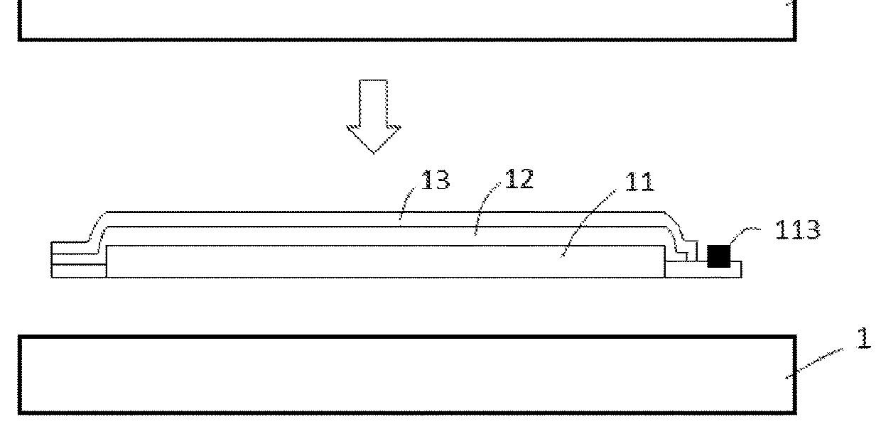
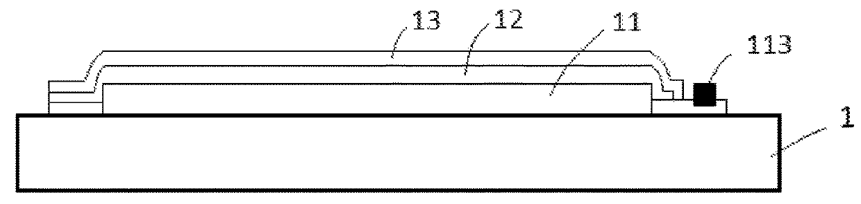
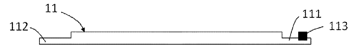
[0026]Referring to FIGS. 1 and 2, the embodiment of the present invention provides a display panel based on flexible OLED, which comprises a flexible substrate 11, an organic light-emitting layer 12 and a thin-film packaging layer 13 are arranged on the flexible substrate 11 sequentially, a first splicing portion 111 is formed on the first side of the flexible substrate 11 by thinning process, a second splicing portion 112 is formed on the second side of the flexible substrate 11 by thinning process, a drive circuit and a control chip 113 are arranged on a part of surface of the first splicing portion 111, the organic light-emitting layer 12 extends to cover the second splicing portion 112.

[0027]In the present embodiment, the second splicing portion 112 and the first splicing portion 111 are formed on the right and left si...


PUM


Abstract

The present invention provides a display panel based on flexible organic light-emitting diode (OLED,) including a flexible substrate, an organic light-emitting layer and a thin-film packaging layer are arranged on the flexible substrate sequentially, a first splicing portion is formed on the first side of the flexible substrate by thinning process, a second splicing portion is formed on the second side of the flexible substrate by thinning process, a drive circuit and a control chip are arranged on a part of surface of the first splicing portion, the organic light-emitting layer extends to cover the second splicing portion. The present invention further provides a seamless splicing display device and a method for manufacturing the same.

Description

BACKGROUND OF THE INVENTION1. Field of the Invention[0001]The present invention relates to a technology of liquid crystal display, and more particularly, to a display panel based on flexible organic light-emitting diode (OLED,) a seamless splicing display device and a method for manufacturing the same.2. The Related Arts[0002]There are two kinds of display splicing, one is the traditional large screen display wall splicing hardware technology, the other is the seamless splicing technology using a projector to achieve by the edge blending technology. Wherein, the wall splicing hardware technology mainly includes: the digital light procession stitching (the gap is less than 0.5 mm,) the cathode ray tube stitching, plasma display panel stitching, and liquid crystal display stitching, but each above-mentioned splicing screen has gaps, the display effect is affected. The seamless splicing technology using the projector, edge fusion, and splicing device can achieve a true seamless splicin...

Claims


Application Information

Patent Timeline
Patent Type & Authority Applications(United States)
IPC IPC(8): H01L27/32H01L51/00H01L51/52H01L51/56
CPCH01L27/3293H01L51/0097H01L51/5253H01L51/56H01L51/003H01L2251/5315H01L2251/5338H01L2227/326H01L21/77H10K59/12H10K59/128Y02E10/549Y02P70/50H10K59/18H10K71/80H10K77/111H10K50/844H10K59/1201H10K2102/311H10K71/00H10K2102/3026
Inventor LIN, BIFEN
Owner SHENZHEN CHINA STAR OPTOELECTRONICS TECH CO LTD
Why Eureka
Try Eureka