Optical fingerprint identification display screen and display device

a fingerprint identification and display screen technology, applied in the field of display technologies, can solve the problems of low signal-noise ratio, limited detection accuracy, and lots of useless information received by the photosensitive transistor after being reflected back, so as to reduce the loss of ridge or valley light before reaching each photosensitive element, improve fingerprint identification accuracy, and avoid interference between the photosensitive elements

Active Publication Date: 2018-07-26
BOE TECH GRP CO LTD +1
View PDF6 Cites 47 Cited by
  • Summary
  • Abstract
  • Description
  • Claims
  • Application Information

AI Technical Summary

Benefits of technology

[0018]Embodiments of this disclosure provide an optical fingerprint identification display screen and a display device. The optical fingerprint identification display screen comprises a counter substrate and an array substrate which are arranged opposite one another. A plurality of photosensitive elements is arranged on a side of the array substrate facing the counter substrate for fingerprint identification. Besides, a mesh-like black matrix layer is arranged on a side of the array substrate facing the counter substrate or on a side of the counter substrate facing the array substrate, wherein mesh regions of the mesh-like black matrix layer correspond to the photosensitive elements. Furthermore, a plurality of light guide members is arranged between each photosensitive element and the counter substrate and at least covers each photosensitive element. Since light guide members are added above the photosensitive elements, and the light guide members and the counter substrate are in contact with each other, light reflected from ridges and valleys of a fingerprint will enter the light guide members maximally after passing through mesh regions of the black matrix layer. Additionally, since the light guide members cover each photosensitive element, light will directly impinge onto the photosensitive elements after refraction within the light guide members. Thus, loss of ridge or valley light before reaching each photosensitive element is reduced. In addition, due to a reflection function of the light guide members and a blocking function of the black matrix layer, interference to the ridge or valley light from display light and ambient light as interference light is shielded. Furthermore, interference between the photosensitive elements is also avoided. Thereby, more accurate fingerprint detection is achieved and the accuracy of fingerprint identification is improved.

Problems solved by technology

In specific implementation, because of interference from ambient light and incident light, in the above optical fingerprint identification device, light received by the photosensitive transistor 003 after being reflected back carries lots of useless information.
This influences detection for fingerprint detection signals and leads to a low signal-noise ratio for signals of such an optical fingerprint identification detection structure.
Thus, the detection accuracy is limited.
In addition, due to a reflection function of the light guide members and a blocking function of the black matrix layer, interference to the ridge or valley light from display light and ambient light as interference light is shielded.

Method used


Image

  • Optical fingerprint identification display screen and display device
  • Optical fingerprint identification display screen and display device
  • Optical fingerprint identification display screen and display device

Examples


Embodiment Construction

[0023]Specific implementations for the optical fingerprint identification display screen and the display device provided by embodiments of this disclosure will be illustrated as follows in detail with reference to the drawings.

[0024]Shapes and sizes of each component in the drawings are not provided to represent the true scale of the display screen, but only for the purpose of illustrating content of this disclosure.

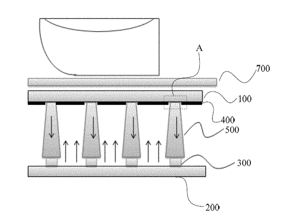
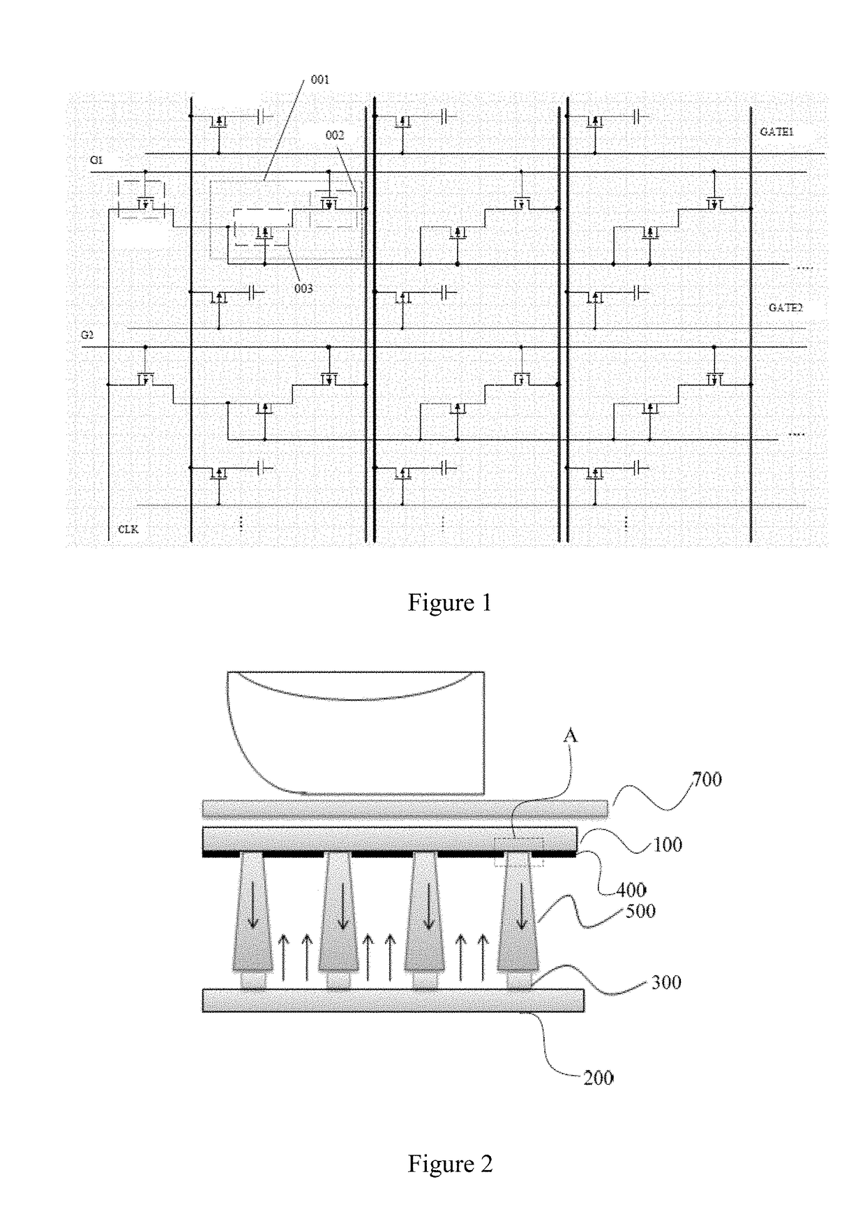
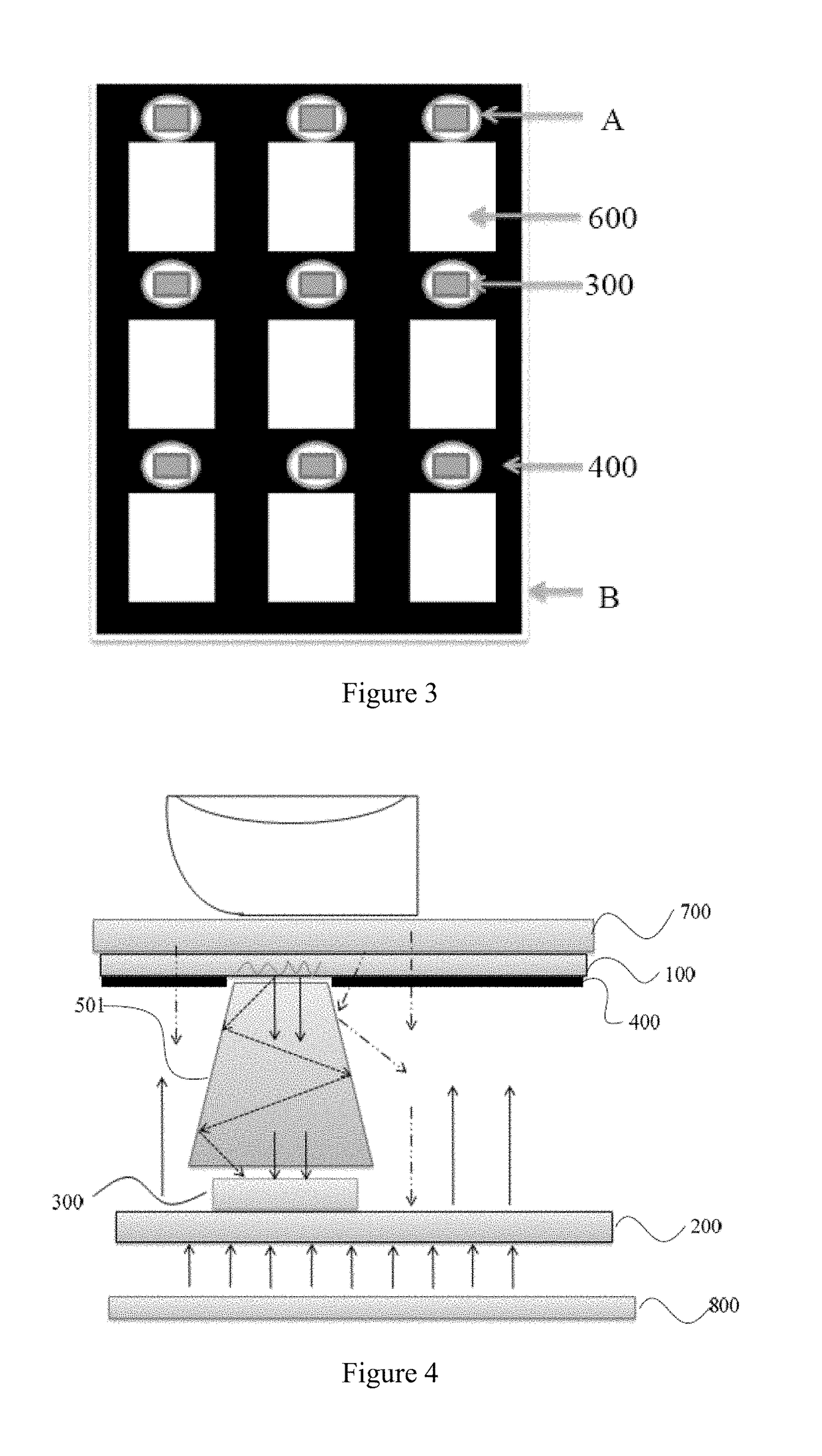
[0025]Embodiments of this disclosure provide an optical fingerprint identification display screen. As shown in FIG. 2, the display screen may comprise a counter substrate 100 and an array substrate 200 which are arranged opposite one another. Additionally, a plurality of photosensitive elements 300 can be arranged on a side of the array substrate 200 facing the counter substrate 100 for fingerprint identification. Additionally, a mesh-like black matrix layer 400 may also be arranged on a side of the array substrate 200 facing the counter substrate 100 or on a side of the...


PUM

PropertyMeasurementUnit
photosensitiveaaaaaaaaaa
refractive indexaaaaaaaaaa
transparentaaaaaaaaaa

Abstract

This disclosure relates to an optical fingerprint identification display screen and a display device. In this disclosure, a plurality of photosensitive elements for fingerprint identification is arranged on an array substrate, such that mesh regions of a mesh-like black matrix layer corresponds to the photosensitive elements. A plurality of light guide members at least covering each of the photosensitive elements is arranged between each photosensitive element and the counter substrate. Since the light guide members and the counter substrate are in contact with each other, light reflected from ridges and valleys of a fingerprint will enter the light guide members maximally after passing through the mesh regions of the black matrix layer, and then directly impinge on the photosensitive elements after refraction within the light guide members.

Description

RELATED APPLICATIONS[0001]The present application is the U.S. national phase entry of PCT / CN2016 / 098043, with an international filling date of Sep. 5, 2016, which claims the benefit of Chinese Patent Application No. 201610004800.X, filed on Jan. 4, 2016, the entire disclosures of which are incorporated herein by reference.FIELD[0002]This disclosure relates to the field of display technologies, and in particular to an optical fingerprint identification display screen and a display device.BACKGROUND ART[0003]In recent years, with rapid development of display technologies, mobile products with biological identification functions have gradually become part of people's life. Particularly, increasing importance has been attached to fingerprinting for its identity uniqueness. Press type and slide type fingerprint identification based on a silicon substrate process has now been integrated into various mobile products. Moreover, future research will also focus on fingerprint identification t...

Claims


Application Information

Patent Timeline
Patent Type & Authority Applications(United States)
IPC IPC(8): G06K9/00H01L27/146G02F1/1333G02F1/1335G02F1/133
CPCG06K9/0004H01L27/14678H01L27/14625H01L27/14623G02F1/13338G02F1/133512G02F1/13306H01L27/156H01L31/16H01L27/3234H01L27/3283H01L27/3246H01L31/1136G02F1/1368G02F2001/13312G02F1/1333G02F1/133374G06V40/1318A61B5/1172G06F3/0412G02F1/13312G02F1/133331H10K59/65H10K59/173H10K59/122
Inventor LIU, WEIDONG, XUECHEN, XIAOCHUANWANG, HAISHENGDING, XIAOLIANGLIU, YINGMINGZHAO, WEIJIEYANG, SHENGJILI, CHANGFENGWANG, PENGPENG
Owner BOE TECH GRP CO LTD
Why Eureka
Try Eureka