Metal Gate Structure

a gate structure and metal technology, applied in the field of integrated circuits, can solve problems such as increasing the complexity of fabricating integrated circuits

Active Publication Date: 2018-08-09
TAIWAN SEMICON MFG CO LTD
View PDF3 Cites 1 Cited by
  • Summary
  • Abstract
  • Description
  • Claims
  • Application Information

AI Technical Summary

Problems solved by technology

As the demand for miniaturization continues, the further shrinking of the process node may increase the complexity of fabricating integrated circuits.

Method used


Image

  • Metal Gate Structure
  • Metal Gate Structure
  • Metal Gate Structure

Examples


Embodiment Construction

[0012]The making and using of the presently preferred embodiments are discussed in detail below. It should be appreciated, however, that the present invention provides many applicable inventive concepts that can be embodied in a wide variety of specific contexts. The specific embodiments discussed are merely illustrative of specific ways to make and use the invention, and do not limit the scope of the invention.

[0013]The present invention will be described with respect to preferred embodiments in a specific context, a metal gate structure for a metal oxide semiconductor (MOS) device. The invention may also be applied, however, to a variety of semiconductor devices.

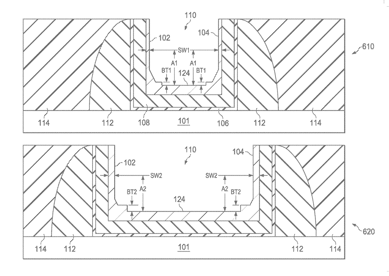
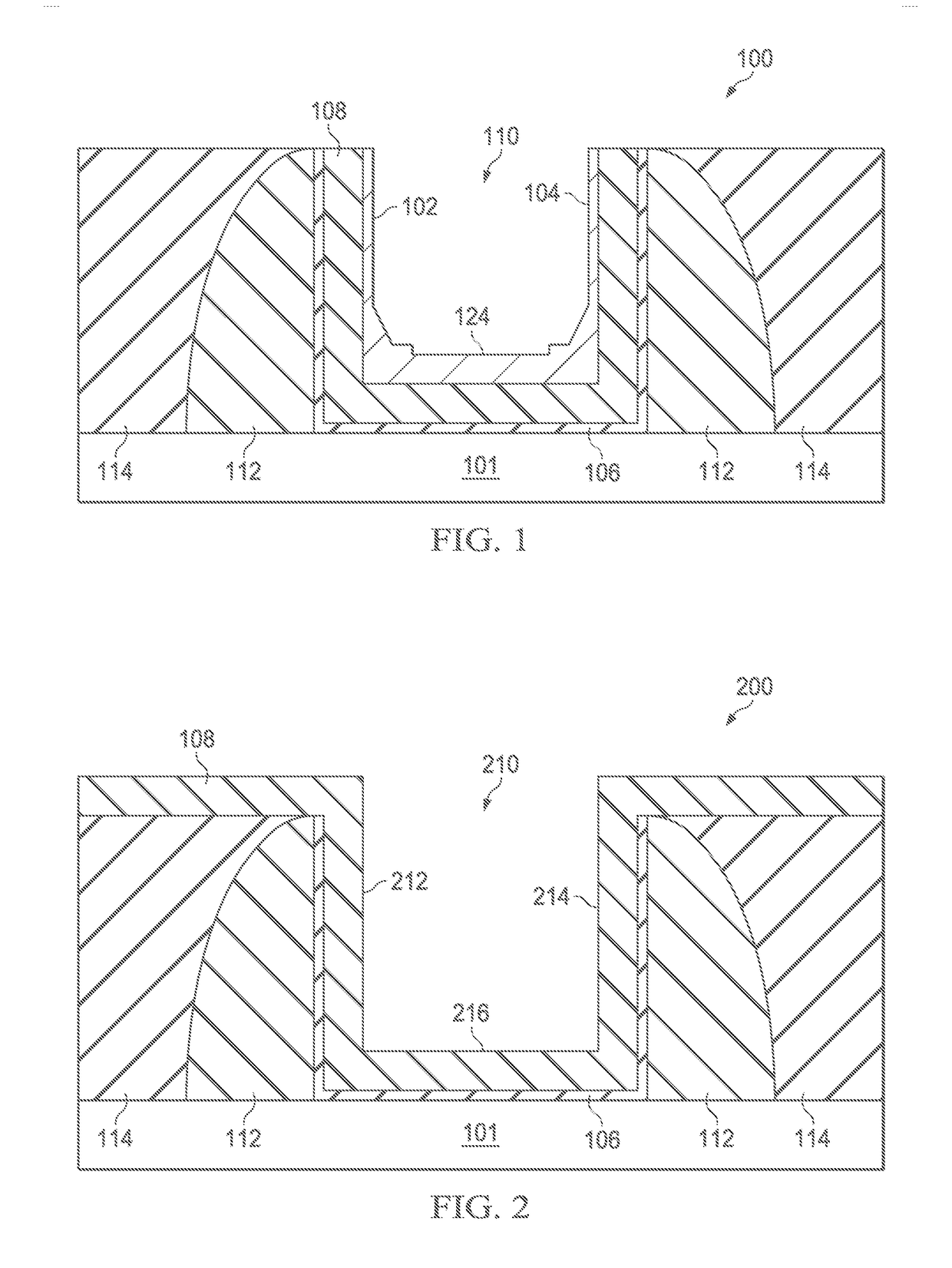
[0014]Referring initially to FIG. 1, a cross sectional view of a metal gate structure is illustrated in accordance with an embodiment. The metal gate structure 100 comprises a trench 110. The trench 110 has a first metal sidewall 102, a second metal sidewall 104 and a metal bottom layer 124. As shown in FIG. 1, the first m...


PUM

PropertyMeasurementUnit
heightaaaaaaaaaa
thicknessaaaaaaaaaa
thicknessaaaaaaaaaa

Abstract

A device comprises a metal gate structure over a substrate, wherein the metal gate structure comprises a first metal sidewall, a metal bottom layer, a first corner portion between the first metal sidewall and the metal bottom layer, wherein the first corner portion comprises a first step and a first ramp, a second metal sidewall and a second corner portion between the second metal sidewall and the metal bottom layer, wherein the second corner portion comprises a second step and a second ramp.

Description

[0001]This is a divisional application of U.S. patent application Ser. No. 15 / 253,383, entitled “Metal Gate Structure” which was filed on Aug. 31, 2016, which is a continuation application of U.S. patent application Ser. No. 14 / 727,162, entitled “Metal Gate Structure” which was filed on Jun. 1, 2015, now U.S. Pat. No. 9,449,832, which is a divisional of U.S. patent application Ser. No. 13 / 214,996, entitled “Metal Gate Structure” which was filed on Aug. 22, 2011 now U.S. Pat. No. 9,048,334, all of which are incorporated herein by reference.BACKGROUND[0002]Since the invention of the integrated circuit, the semiconductor industry has experienced rapid growth due to improvements in the integration density of a variety of electronic components (e.g., transistors, diodes, resistors, capacitors, etc.). This improvement in integration density has come from shrinking the semiconductor process node (e.g., shrink the process node towards the sub-20 nm node). As the demand for miniaturization c...

Claims


Application Information

Patent Timeline
Patent Type & Authority Applications(United States)
IPC IPC(8): H01L29/423H01L21/8234H01L21/28H01L29/49H01L21/311H01L21/285H01L29/51
CPCH01L21/31105H01L29/513H01L29/42376H01L21/285H01L21/2855H01L21/28114H01L21/28247H01L29/517H01L21/823456H01L29/4236H01L29/4966
Inventor LIM, PENG-SOONLEE, DA-YUANHSU, KUANG-YUAN
Owner TAIWAN SEMICON MFG CO LTD
Why Eureka
Try Eureka