

OLED pixel driving circuit and pixel driving method
Patent Information
- Authority / Receiving Office
- US · United States
- Patent Type
- Applications(United States)
- Current Assignee / Owner
- SHENZHEN CHINA STAR OPTOELECTRONICS SEMICON DISPLAY TECH CO LTD
- Publication Date
- 2018-10-18
- Estimated Expiration
- Not applicable · inactive patent
Smart Images

Figure 1 
Figure 2 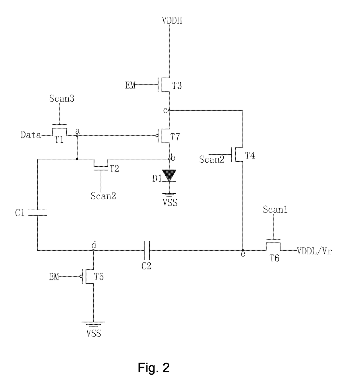
Figure 3
Abstract
Description
FIELD OF THE INVENTION
[0001] The present invention relates to a display technology field, and more particularly to an OLED pixel driving circuit and a pixel driving method.BACKGROUND OF THE INVENTION
[0002] The Organic Light Emitting Display (OLED) possesses many outstanding properties of self-illumination, low driving voltage, high luminescence efficiency, short response time, high clarity and contrast, near 180° view angle, wide range of working temperature, applicability of flexible display and large scale full color display. The OLED is considered as the most potential display device.
[0003] The OLED is a current driving element. When the electrical current flows through the organic light emitting diode, the organic light emitting diode emits light, and the brightness is determined according to the current flowing through the organic light emitting diode itself. Most of the present Integrated Circuits (IC) only transmit voltage signals. Therefore, the OLED pixel driving circuit needs...