Dual interface metal smart card with booster antenna

a metal smart card and booster technology, applied in the structure of radiating elements, instruments, and the details of semiconductor/solid-state devices, can solve the problems of useless contactless smart cards, and achieve the effect of enhancing rf transmission

Active Publication Date: 2018-10-25
COMPOSECURE LLC
View PDF1 Cites 22 Cited by
  • Summary
  • Abstract
  • Description
  • Claims
  • Application Information

AI Technical Summary

Benefits of technology

This patent describes an electronic card that includes a metal layer with two openings containing an integrated circuit module and a plug made of non-RF-impling material. There are also some components placed between these openings including a ferritte layer and a booster antenna. These technical features allow for secure communication without being affected by external factors like weather or distance.

Problems solved by technology

The technical problem addressed in this patent text is how to make dual interface (contactless and contact) smart cards with a metal layer that minimizes interference with RF communication signals and has an aesthetically pleasing interface with the card surface.

Method used


Image

  • Dual interface metal smart card with booster antenna
  • Dual interface metal smart card with booster antenna
  • Dual interface metal smart card with booster antenna

Examples


Embodiment Construction

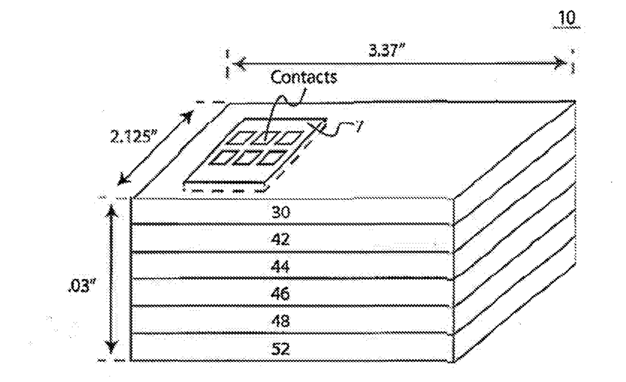
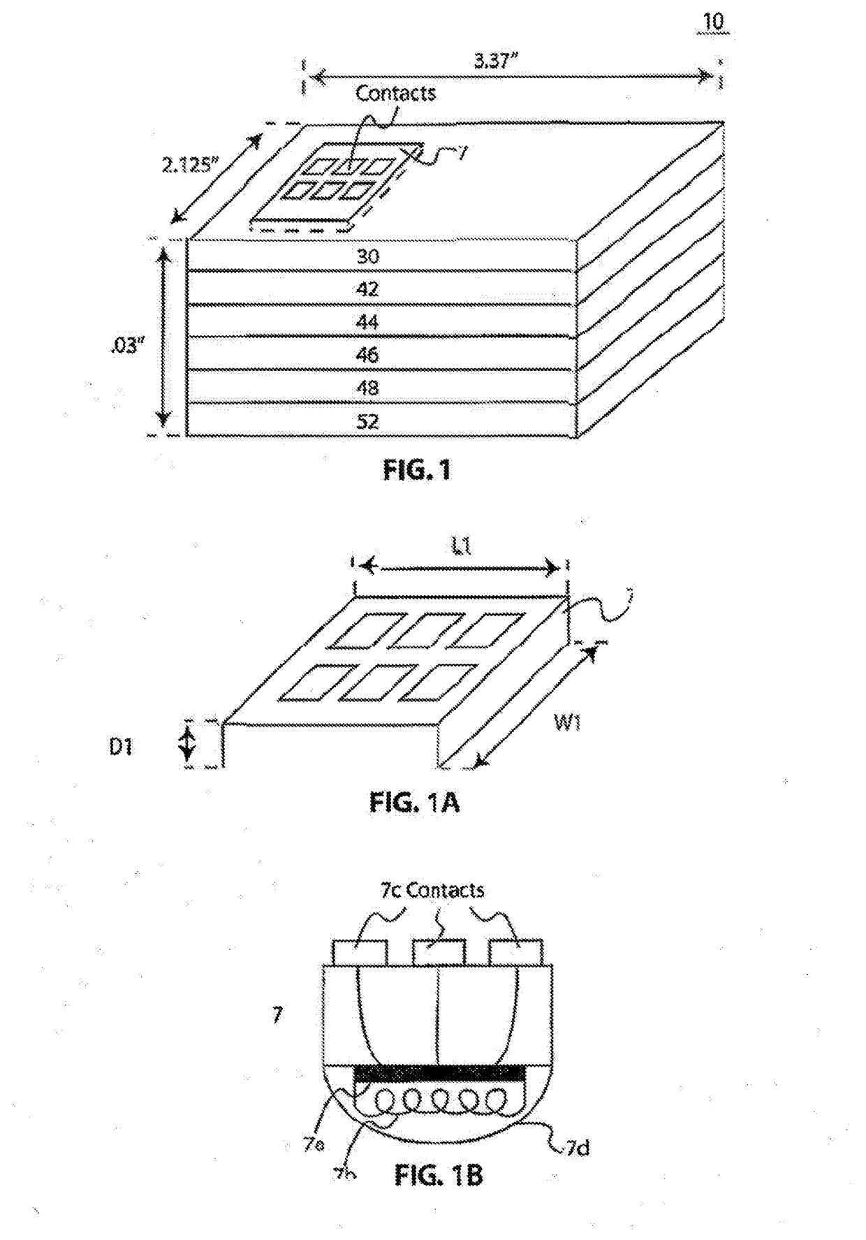
[0038]An integrated circuit (IC) module 7 having multiple contacts as shown in FIG. 1A is to be mounted in, and on, a card 10 as shown in FIG. 1 with the top surface of the IC module and its contacts generally flush with the top surface of the card. By way of example it is shown that the length, width and depth of the card may respectively be approximately 3.37 inches by 2.125 inches by 0.03 inches. For purpose of illustration and the discussion to follow, we assume, as shown in FIG. 1A, that the IC module has a depth D1, a length L1 and a width W1. Modules such as IC module 7 are commercially available, for example, from Infineon or NXP. The lateral dimensions of some of these modules were approximately 0.052 inches by 0.47 inches with a depth ranging from 0.005 inches to more than 0.025 inches. These dimensions are purely illustrative and IC modules used to practice the invention may be greater or smaller in size.

[0039]As shown in FIG. 1B, IC module 7 contains an internal micropro...


PUM


Abstract

A card having a metal layer and an opening or cut-out region in the metal layer, with a dual-interface integrated circuit (IC) module disposed in the opening or cut-out region. A ferrite layer is disposed below the metal layer and a booster antenna is attached to the ferrite layer. A vertical hole extends beneath the IC module through the ferrite layer. The booster antenna may be physically connected to the IC module or may be configured to inductively couple to the IC module. In some embodiments, the IC may be disposed in or on a non-conductive plug disposed within the opening or cut-out region, or the vertical hole may have a non-conductive lining, or a connector may be disposed between the booster antenna and the IC module in the vertical hole.

Description


Claims


Application Information

Patent Timeline
Owner COMPOSECURE LLC
Why Eureka
Try Eureka