Terminal fitting and connector
- Summary
- Abstract
- Description
- Claims
- Application Information
AI Technical Summary
Benefits of technology
Problems solved by technology
Method used
Image
Examples
embodiment 1
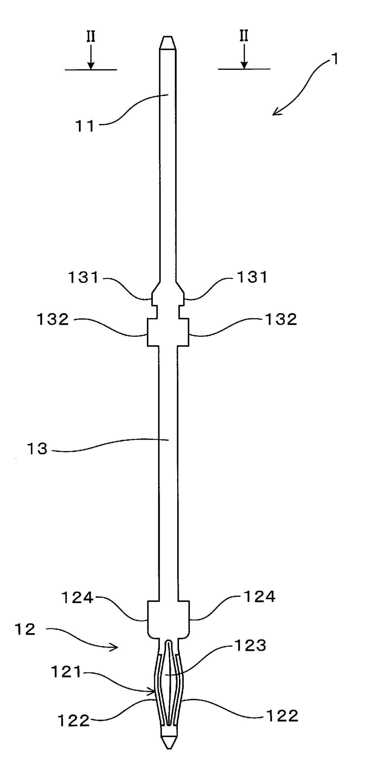
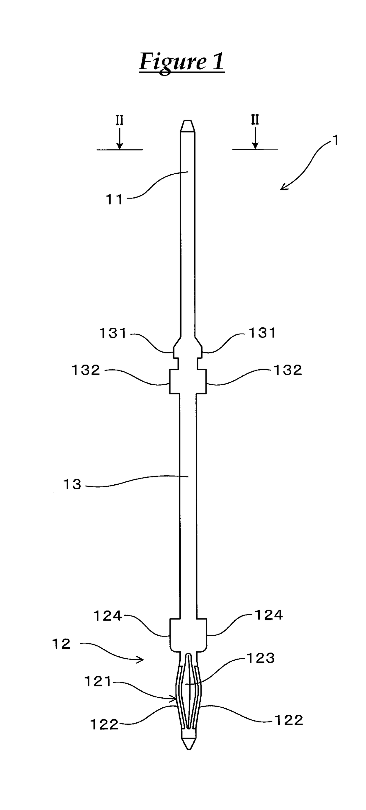
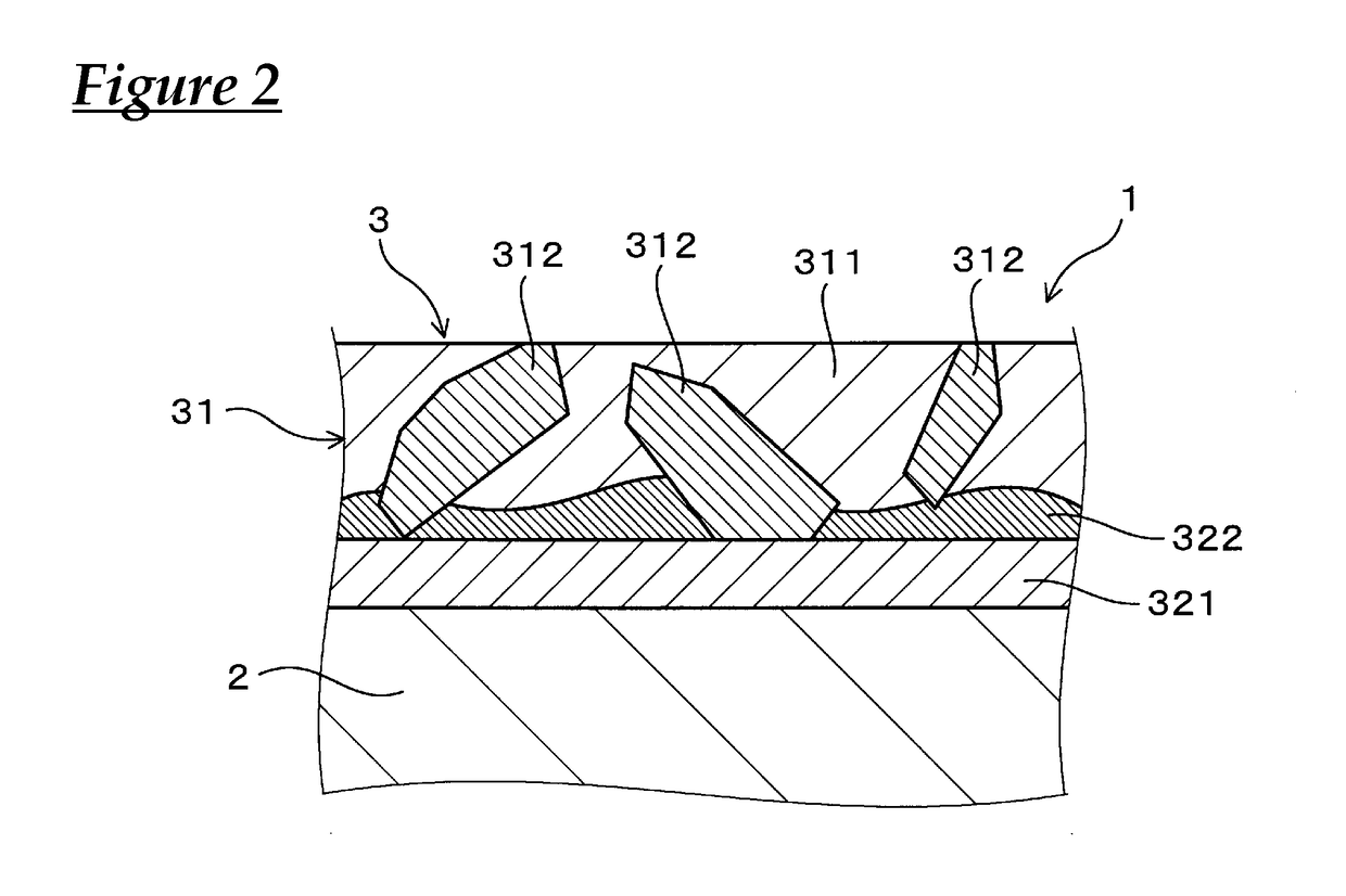
[0052]The terminal fitting according to Embodiment 1 will be described with reference to FIGS. 1 to 5. As shown in FIGS. 1 to 5, a terminal fitting 1 of the present embodiment includes a metal base material 2, and a plating film 3 that covers a surface of the metal base material 2. The plating film 3 has an outermost layer 31 that is exposed at the outermost surface. The outermost layer 31 includes an intermetallic compound 312.
[0053]The plating film 3 includes a Ni foundation layer 321 that is formed on the surface of the metal base material 2, and the outermost layer 31 that is formed above the Ni foundation layer 321, and is exposed at the outermost surface of the plating film 3. The outermost layer 31 includes a Sn parent phase 311, and the intermetallic compound 312 that is dispersed in the Sn parent phase 311.
[0054]In the present embodiment, the metal base material 2 is specifically a Cu alloy. Furthermore, the intermetallic compound 312 is made of (Ni0.4Pd0.6)Sn4. The particl...
experimental examples
[0067]Hereinafter, more specific description will be given with reference to experimental examples.
[0068]Sample 1 was produced by sequentially forming a Ni plating film (thickness: 1 μm), a Pd plating film (thickness: 0.02 μm), and a Sn plating film (thickness: 1.5 μm) on a surface of a Cu alloy plate material, and then subjecting the resultant to reflow processing at 350° C.
[0069]Sample 2 was produced in the same manner as in Sample 1 but using a Pd plating film (thickness: 0.025 μm), and a Sn plating film (thickness: 1.25 μm) instead. Furthermore, Sample 3 was produced in the same manner as in Sample 1 but using a Pd plating film (thickness: 0.03 μm) and a Sn plating film (thickness: 1.0 μm) instead. Note that for comparison, Sample 1C was produced by sequentially forming a Ni plating film (thickness: 1 μm), and a Sn plating film (thickness: 1 μm) on a surface of a Cu alloy plate material, and then subjecting the resultant to reflow processing at 350° C.
[0070]Then, cross-sections ...
PUM
 Abstract
Description
Claims
Application Information


