Terahertz detector comprised of p-n junction diode

a detector and diode technology, applied in the field of high-frequency detectors, can solve the problems of high flicker noise in mosfets and the upper limit of operation frequency, and achieve the effect of higher signal-to-noise ratio (snr) and higher operation frequency

Active Publication Date: 2018-11-15
INT BUSINESS MASCH CORP
View PDF5 Cites 0 Cited by
  • Summary
  • Abstract
  • Description
  • Claims
  • Application Information

AI Technical Summary

Benefits of technology

[0009]Techniques of the present invention can provide substantial beneficial technical effects. By way of example only and without limitation, one or more embodiments may provide one or more of the following advantages, among other benefits:[0010]substantially lower effective diffusion capacitance;[0011]lower effective series resistance;[0012]substantially higher signal-to-noise ratio;[0013]mechanical flexibility.

Problems solved by technology

The higher flicker noise in MOSFETs is often attributed to the presence of interface states between the gate dielectric and the channel of the transistor.
However, an upper limit of the operation frequency is still dictated, to a large extent, by an effective path length for carrier diffusion and an effective series resistance of the diode.

Method used


Image

  • Terahertz detector comprised of p-n junction diode
  • Terahertz detector comprised of p-n junction diode
  • Terahertz detector comprised of p-n junction diode

Examples


Embodiment Construction

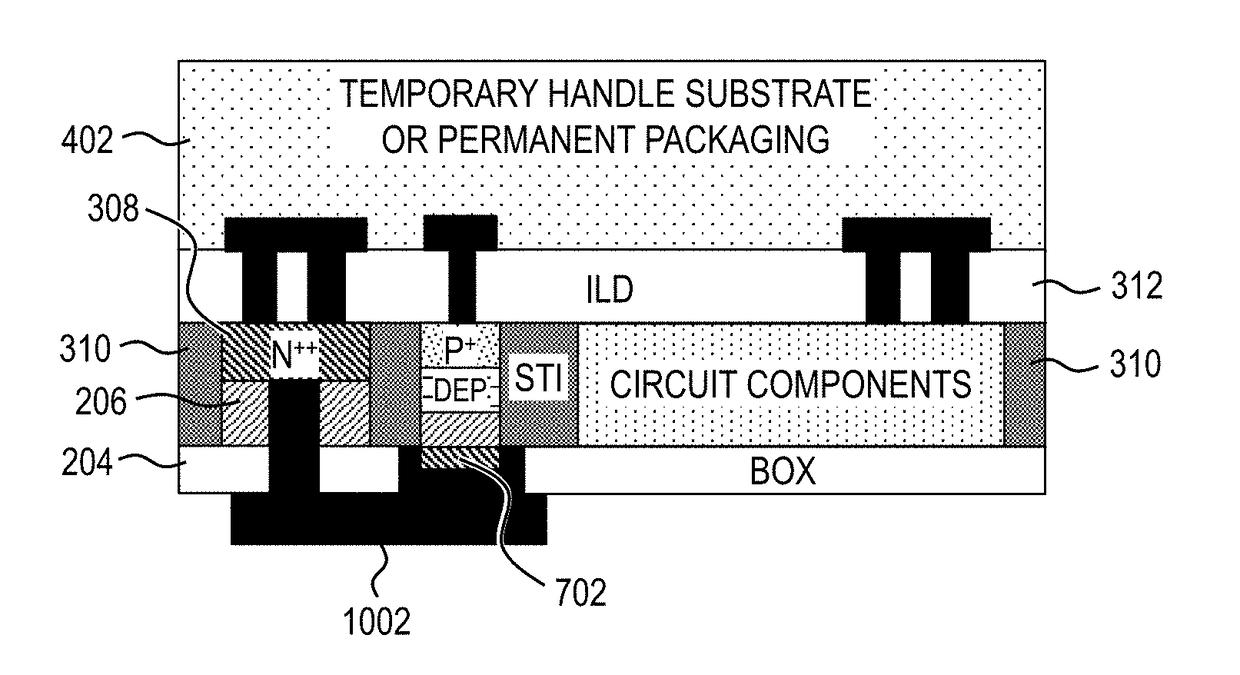
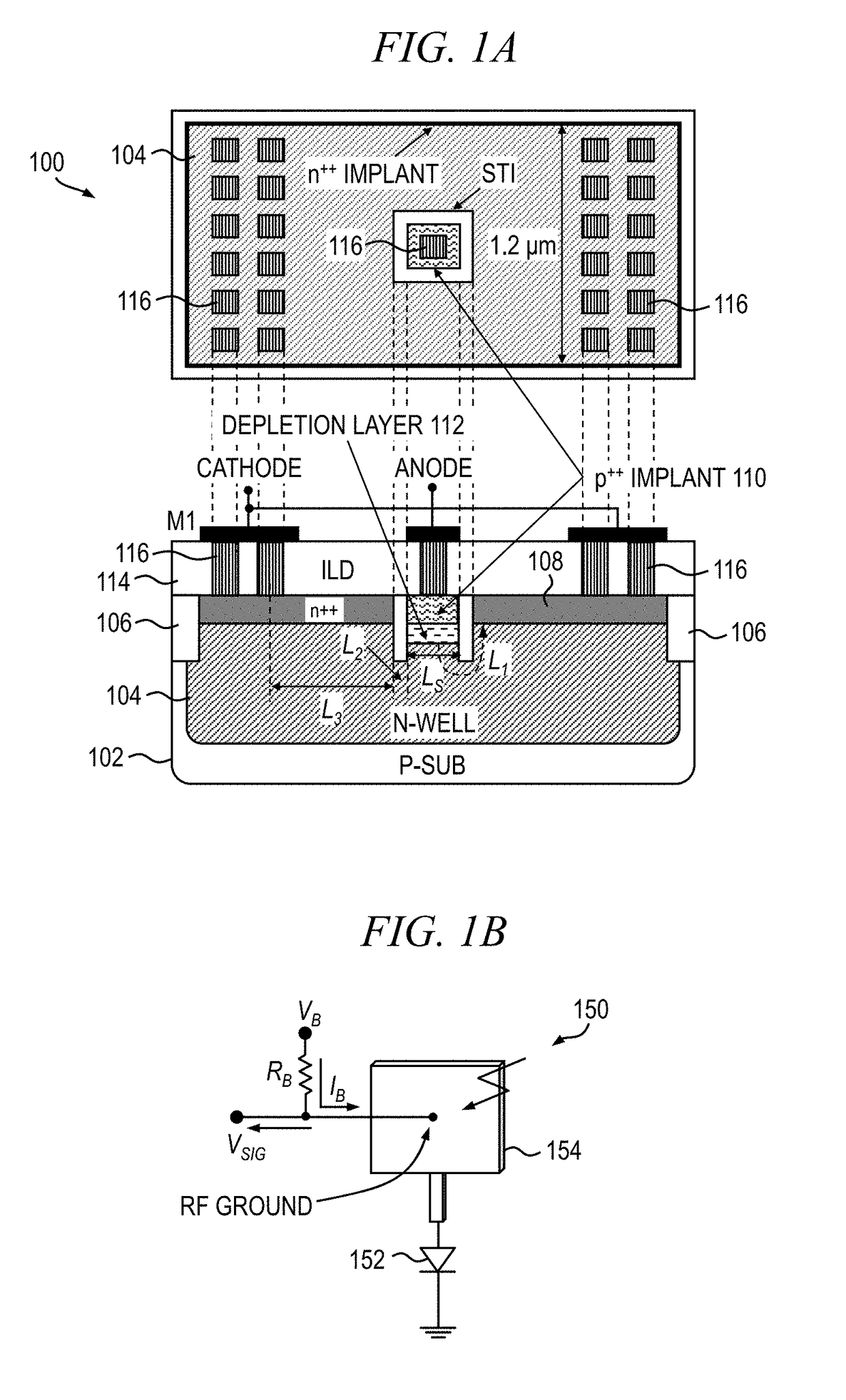
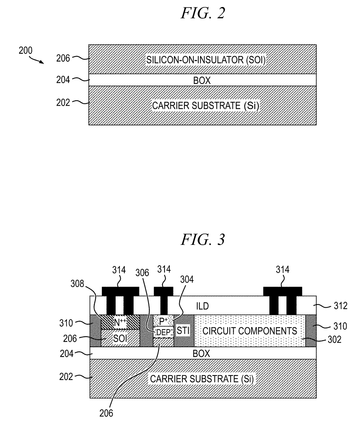
[0023]Principles of the present invention will be described herein in the context of illustrative detector devices comprised of p-n junction diodes and applications utilizing such detector devices. It is to be appreciated, however, that the specific structures, circuits and / or methods illustratively shown and described herein are to be considered exemplary as opposed to limiting. Moreover, it will become apparent to those skilled in the art given the teachings herein that numerous modifications can be made to the embodiments shown that are within the scope of the appended claims. That is, no limitations with respect to the embodiments shown and described herein are intended or should be inferred.

[0024]Although the overall fabrication method and the structures for the disclosed embodiments are entirely novel, certain individual processing steps required to implement the device may utilize conventional semiconductor fabrication techniques and conventional semiconductor fabrication too...


PUM


Abstract

A method of forming a semiconductor detector including: forming a p-n junction diode in an active device layer of a silicon-on-insulator (SOI) substrate, the active device layer being formed on an insulator layer of the SOI substrate; forming a first opening through the insulator layer to access a backside of a first doped region of the diode, the first doped region underlying a second doped region of the diode; forming a back contact on a back surface of the first doped region and electrically connecting with the first doped region; forming a conductive interconnect layer on an upper surface of the SOI substrate, the interconnect layer including a first top contact providing electrical connection with the second doped region; and forming an electrode in the first opening on the backside of the detector structure, the electrode providing electrical connection with the back contact of the diode.

Description

CROSS-REFERENCE TO RELATED APPLICATIONS[0001]This patent application is a divisional of U.S. patent application Ser. No. 15 / 484,172 filed Apr. 11, 2017, entitled “TERAHERTZ DETECTOR COMPRISED OF P-N JUNCTION DIODE,” the complete disclosure of which is expressly incorporated herein by reference in its entirety for all purposes.BACKGROUND OF THE INVENTION[0002]The present invention relates generally to the electrical, electronic and computer arts, and, more particularly, to high-frequency detectors.[0003]It has been demonstrated that high-frequency (e.g., terahertz (THz)) detectors based on p-n junction diodes provide certain benefits over diode-connected metal-oxide-semiconductor (MOS) transistors and heterojunction bipolar transistors (HBTs) due to their higher corner frequency, fc. Flicker noise, also referred to as 1 / f noise, is often characterized by the corner frequency between the region dominated by the low-frequency flicker noise and the higher-frequency “flat-band” noise. MO...

Claims


Application Information

Patent Timeline
Patent Type & Authority Applications(United States)
IPC IPC(8): H01L23/66H01L29/16H01L29/861H01L29/06H01L21/762H01L21/324H01L21/02H01L29/66H01L21/265
CPCH01L29/16H01L29/861H01L29/0649H01L21/76264H01L21/324H01L23/66H01L21/0262H01L21/02576H01L21/02532H01L29/66136H01L21/26513H01L21/02488H01L21/02579H01L29/8613H01L27/1203H01L31/103H01L31/1896H01L31/00
Inventor HEKMATSHOARTABARI, BAHMANSHAHIDI, GHAVAM G.
Owner INT BUSINESS MASCH CORP
Why Eureka
Try Eureka