Semiconductor memory device

a memory device and semiconductor technology, applied in semiconductor devices, digital storage, instruments, etc., can solve the problems of rc delay and inability to achieve high-speed operation, and achieve the effect of capacitan

Active Publication Date: 2006-09-14
RENESAS ELECTRONICS CORP +11
View PDF4 Cites 0 Cited by
  • Summary
  • Abstract
  • Description
  • Claims
  • Application Information

AI Technical Summary

Benefits of technology

[0014]FIG. 6 is characteristic view showing a change of an effective capacitance with respect to a gate voltage of an MOS transistor;
[0015]FIG. 7 is a characteristic view showing an effective capacitance in a variety of gate voltage ranges in an MOS transistor;

Problems solved by technology

Losing signal energy (total amount of charge) flowing through the word line and bit line results in an RC delay, and a high speed operation is inhibited.

Method used


Image

  • Semiconductor memory device
  • Semiconductor memory device
  • Semiconductor memory device

Examples


first embodiment

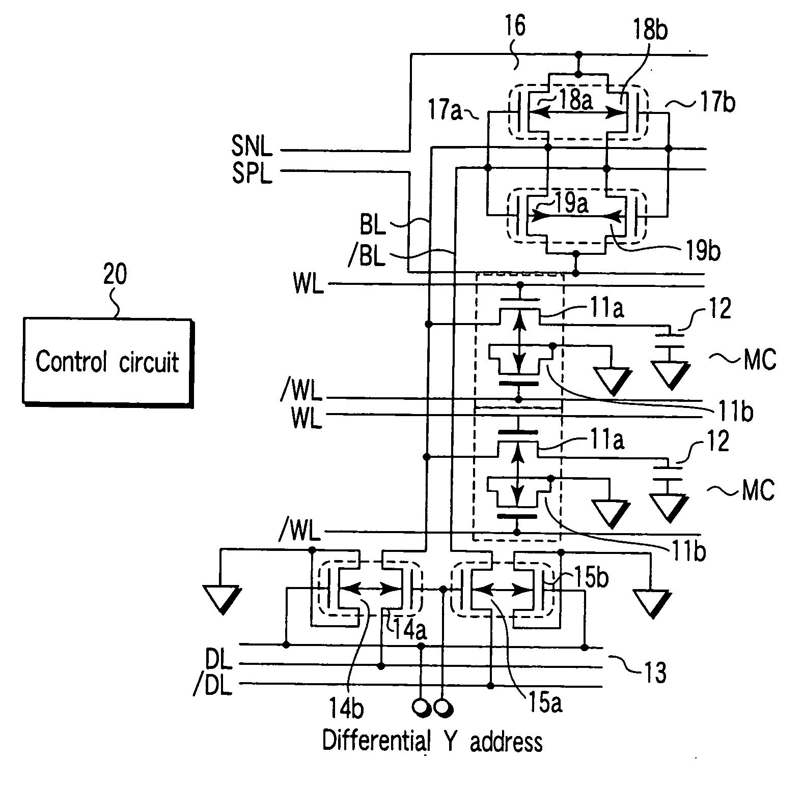
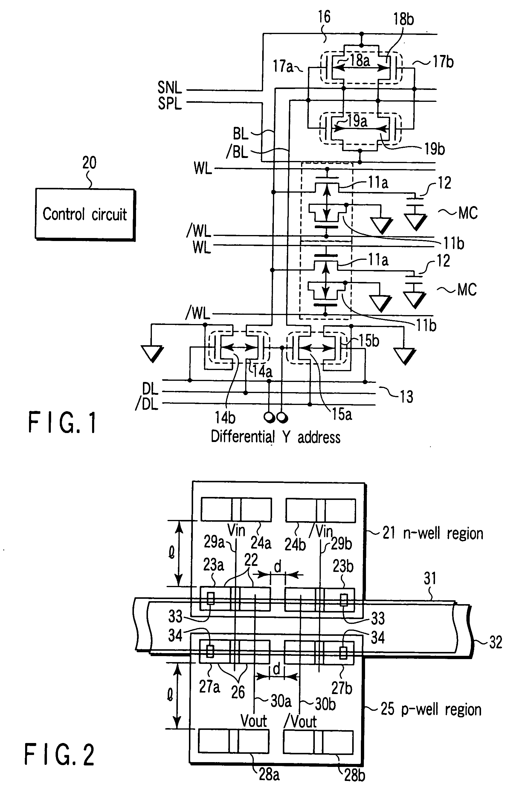
[0023]FIG. 1 is a circuit diagram showing a DRAM according to a first embodiment. In the figure, WL and / WL denote differential word lines, and BL and / BL denote differential bit lines. Memory cells MC are allocated to cross points of the differential word lines WL and / WL and the differential bit lines BL and / BL, respectively. The memory cells MC are connected to the corresponding word lines WL and / WL and differential bit lines BL and / BL, respectively.

[0024] In this embodiment, each memory cell MC includes nMOS transistors 11a and 11b for a transfer gate constituting paired transistors, and one capacitor 12 for data storage connected to one nMOS transistor lla of the nMOS transistors 11a and 11b.

[0025] A gate electrode of the nMOS transistor 11a in the memory cell MC is connected to one word line WL of the differential word lines, and a drain of the nMOS transistor 11a is connected to one bit line BL of the differential bit lines. The capacitor 12 is connected between a source...

second embodiment

[0094] Now, a case in which the present invention is applied to an SRAM will be described here.

[0095]FIG. 13 shows a circuit configuration of the SRAM according to the second embodiment. In the figure, WL and / WL denote differential word lines, and BL and / BL denote differential bit lines. Memory cells MC are allocated at cross points of the differential word lines WL, / WL and the differential bit lines BL, / BL. The memory cells MC are connected to the differential word lines WL, / WL and differential bit lines BL, / BL.

[0096] A plurality of differential word lines and a plurality of differential bit lines are provided in the SRAM according to the embodiment. Memory cells MC are allocated at cross points of the plurality of differential word lines WL, / WL and the plurality of differential bit lines BL, / BL, respectively. FIG. 13 shows only one memory cell from among them.

[0097] In addition to the memory cells MC, as is the case with the DRAM shown in FIG. 1, there are provided a co...


PUM


Abstract

A memory cell MC includes nMOS transistors for a transfer gate configured to be paired with each other, and one capacitor for data storage connected to the nMOS transistor. A gate electrode of the nMOS transistor is connected to a word line WL, and a drain is connected to a bit line BL. A gate electrode of the nMOS transistor is connected to a word line /WL, and a drain and a source are connected to a ground. The capacitor is connected between a source of the nMOS transistor and the ground. A Y selector circuit is connected between a differential bit line BL, /BL and a differential data line DL, /DL. The Y selector circuit has two pairs of nMOS transistors configured to be paired transistors, respectively.

Description

CROSS-REFERENCE TO RELATED APPLICATIONS [0001] This application is based upon and claims the benefit of priority from prior Japanese Patent Application No. 2005-050632, filed Feb. 25, 2005, the entire contents of which are incorporated herein by reference. BACKGROUND OF THE INVENTION [0002] 1. Field of the Invention [0003] The present invention relates to a semiconductor memory device such as a dynamic random access memory (DRAAM) or a static random access memory (SRAM), and particularly, to a semiconductor memory device capable of achieving a high speed operation. [0004] 2. Description of the Related Art [0005] In a semiconductor memory device such as a DRAM or an SRAM, a signal is transmitted in a memory mat at a comparatively long distance of a word line and a bit line. Therefore, a timing margin caused by an RC delay in the word line and bit line must be significantly taken. When a line such as the word line or bit line is regarded as a transmission line, this line is released f...

Claims


Application Information

Patent Timeline
Patent Type & Authority Applications(United States)
IPC IPC(8): G11C7/00
CPCG11C5/063G11C7/12G11C7/18G11C11/405G11C11/4094G11C11/4097H01L27/108H10B12/00H01L27/105
Inventor OTSUKA, KANJIUSAMI, TAMOTSU
Owner RENESAS ELECTRONICS CORP
Why Eureka
Try Eureka