Pixel circuit and image sensor including thereof

a pixel circuit and image sensor technology, applied in the field of image sensors, can solve problems such as dynamic range, and achieve the effect of easy embodied

Active Publication Date: 2018-11-29
SAMSUNG ELECTRONICS CO LTD
View PDF2 Cites 22 Cited by
  • Summary
  • Abstract
  • Description
  • Claims
  • Application Information

AI Technical Summary

Benefits of technology

[0005]The present disclosure provides a pixel circuit which is easily embodied and provides a wide dynamic range under various illumination conditions, and provides an image sensor including the pixel circuit.

Problems solved by technology

In relation to quality of an image sensor, a dynamic range can be problematic, and when a wide dynamic range (WDR) is provided, both a bright region and a dark region of an image may be expressed in detail.

Method used


Image

  • Pixel circuit and image sensor including thereof
  • Pixel circuit and image sensor including thereof
  • Pixel circuit and image sensor including thereof

Examples


Embodiment Construction

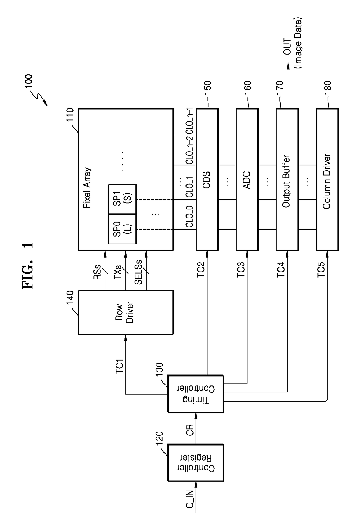
[0024]It will be understood that, although the terms first, second, third etc. may be used herein to describe various elements, these elements should not be limited by these terms. Unless indicated otherwise, these terms are generally used to distinguish one element from another. Thus, a first element discussed below in one section of the specification could be termed a second element in a different section of the specification without departing from the teachings of the present disclosure. Also, terms such as “first” and “second” may be used in the claims to name an element of the claim, even thought that particular name is not used to describe in connection with the element in the specification.

[0025]The embodiments are described, and illustrated in the drawings, in terms of functional blocks and / or units. These blocks and / or units may be physically implemented by electronic (or optical) circuits such as logic circuits, discrete components, microprocessors, hard-wired circuits, me...


PUM


Abstract

An image sensor includes a pixel array including a first shared pixel and a second shared pixel that are adjacent to each other in a row direction. The first shared pixel includes two or more photo diodes in a first row and two or more photo diodes in a second row, and the first shared pixel includes a first floating diffusion region shared by the photo diodes of the first shared pixel. The second shared pixel includes two or more photo diodes in the first row and two or more photo diodes in the second row, and the second shared pixel includes a second floating diffusion region shared by the photo diodes of the second shared pixel.

Description

CROSS-REFERENCE TO RELATED APPLICATION[0001]This application claims the benefit of Korean Patent Application No. 10-2017-0064388, filed on May 24, 2017, in the Korean Intellectual Property Office, the disclosure of which is incorporated herein in its entirety by reference.BACKGROUND[0002]The present disclosure relates to an image sensor, and more particularly, to an image sensor including a pixel circuit including a shared pixel.[0003]Image sensors that capture an image and convert it into an electrical signal are used in cameras installed in, for example, vehicles, security devices, and robots as well as in consumer electronics such as digital cameras, cameras for mobile phones, and portable camcorders. Such image sensors may include a pixel array, and each pixel included in the pixel array may include a photo detecting device. The photo detecting device may generate an electrical signal depending on intensity of the absorbed light.[0004]Sizes of pixels of image sensors have been g...

Claims


Application Information

Patent Timeline
Patent Type & Authority Applications(United States)
IPC IPC(8): H04N5/355H04N5/3745
CPCH04N5/3559H04N5/3745H04N5/35581H04N23/54H04N23/73H04N25/57H04N25/583H04N25/77H04N25/134H04N23/70H04N25/59H04N25/589
Inventor HWANG, MIN-JILEE, SEUNG-JINLEE, YOUNG-WOOHONG, SEOK-YONG
Owner SAMSUNG ELECTRONICS CO LTD
Why Eureka
Try Eureka